


Quick Research
Generate reliable direction feasibility study reports for your R&D in just a few steps.

Technical Q&A
Discover and master advanced knowledge NOW. Basics, ideas, possibilities, all at once.

Find Solutions
As an expert in R&D theories, this can generate solutions to your technical problems instantly.

Evaluate Feasibility
Analyze your overall solution with one click, know your potential R&D risks in advance.

Monitor Landscape
Get weekly tech updates, stay abreast of the latest tech innovations and key insights.
Thin film transistor array substrate and preparation method thereof
一种薄膜晶体管、阵列基板的技术,应用在薄膜晶体管阵列基板及其制备领域,能够解决刻蚀液损伤、薄膜晶体管电学特性稳定性劣化等问题,达到提升稳定性、避免不良影响的效果
- Summary
- Abstract
- Description
- Claims
- Application Information
AI Technical Summary
Problems solved by technology
Method used
Image

Examples
Embodiment 1
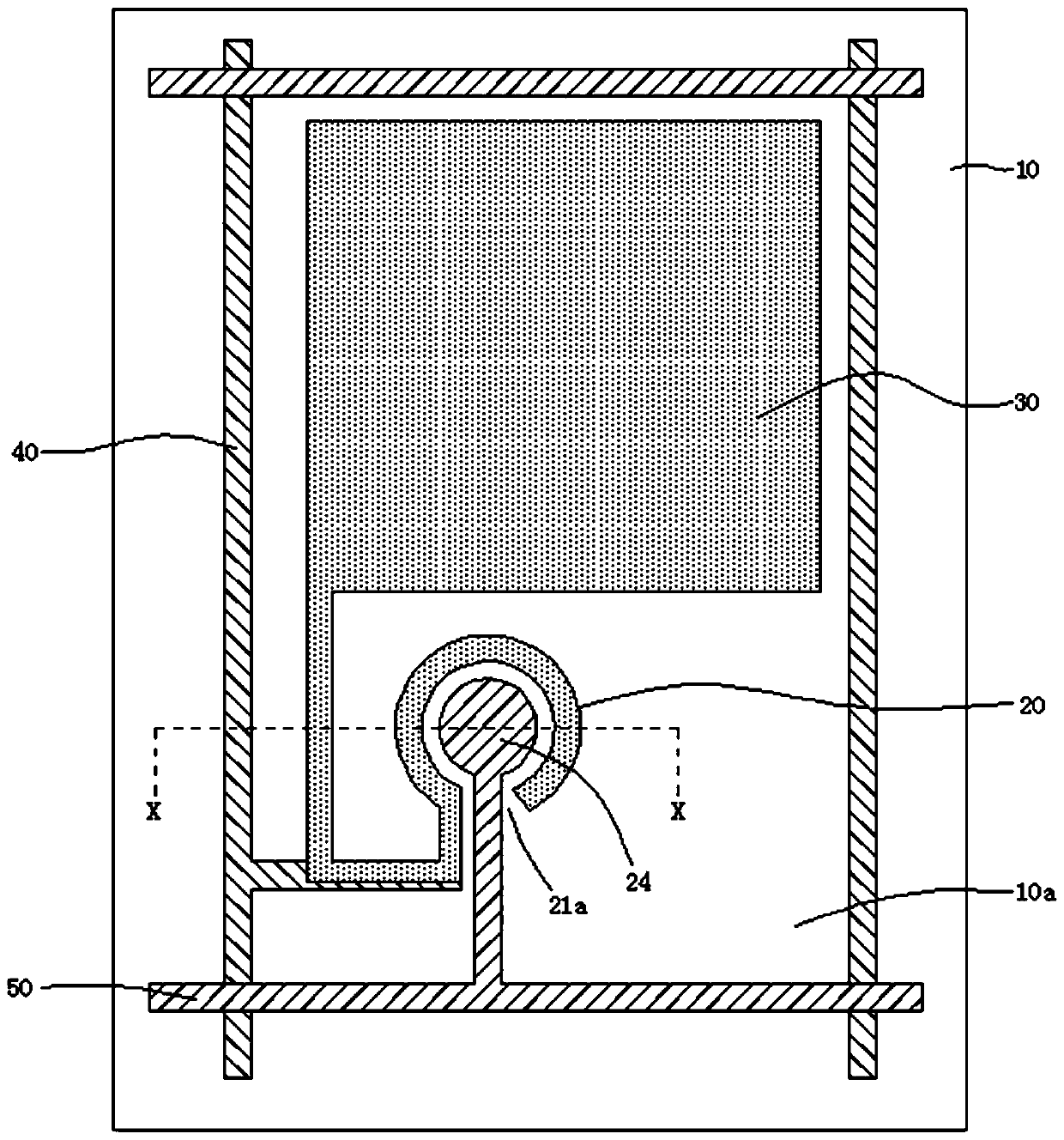
[0048] This embodiment first provides a thin film transistor array substrate, see figure 2 with image 3 ,among them, figure 2 Is a schematic diagram of the planar structure of the thin film transistor array substrate, image 3 Yes figure 2 A cross-sectional view along the X-X line, and figure 2 The insulating layer in the array substrate is not shown in. Such as figure 2 with image 3 As shown, the thin film transistor array substrate includes a pixel unit 10a defined by the intersection of a data line 40 and a gate line 50. The pixel unit 10a is provided with a thin film transistor 20 and a pixel electrode 30. The thin film transistor 20 and the The pixel electrodes 30 are electrically connected to each other.
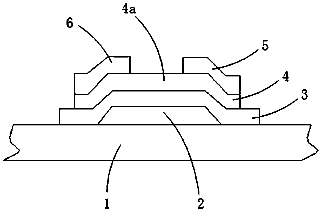
[0049] The thin film transistor 20 includes a source electrode 21, a first insulating layer 22, a semiconductor active layer 23, a gate electrode 24 and a drain electrode 25 formed on the base substrate 10. Specifically, the source electrode 21 is formed on the bas...
Embodiment 2
[0072] As the use time of the thin film transistor array substrate increases, the threshold voltage of the thin film transistor on the array substrate will drift, resulting in poor electrical characteristics of the thin film transistor. For this reason, this embodiment provides another method on the basis of Embodiment 1. A thin film transistor array substrate.
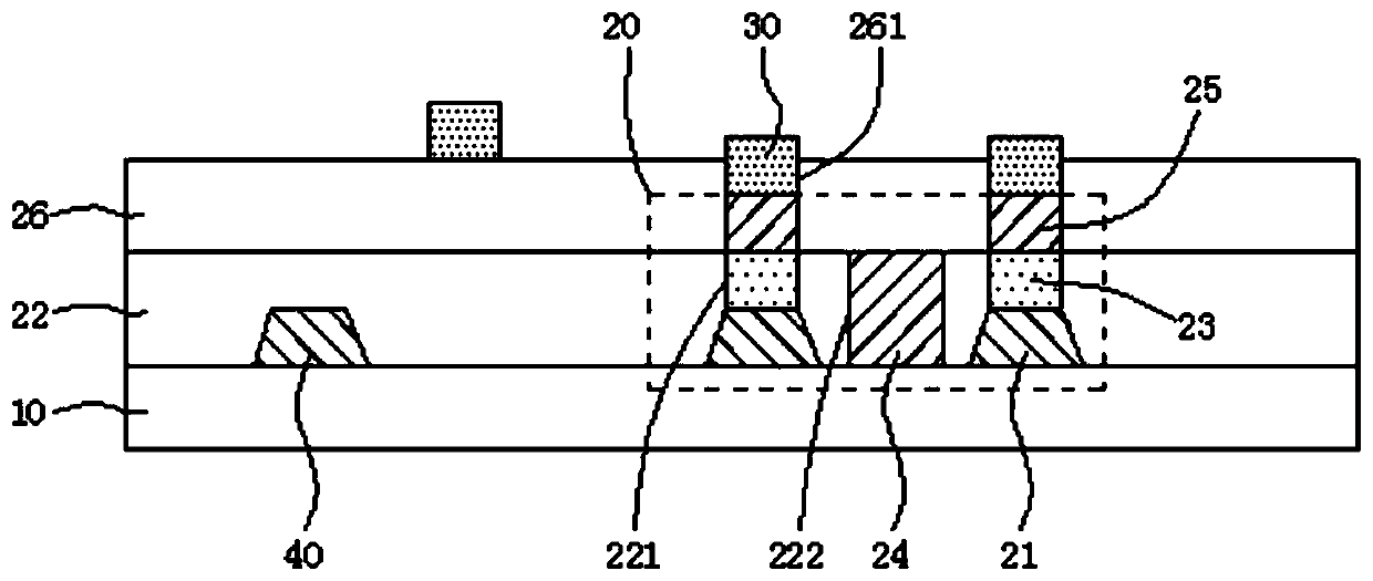
[0073] Refer to Figure 5 with Image 6 The difference between the thin film transistor array substrate provided in this embodiment and the first embodiment is that in this embodiment, the thin film transistor 20 further includes a sub-gate electrode 27, and the array substrate further includes a sub-gate line 60.
[0074] Specifically, such as Figure 5 with Image 6 On the basis of embodiment 1, a gate groove 223 is further provided in the first insulating layer 22, the gate groove 223 surrounds the outer side of the annular groove 221, and the secondary gate electrode 27 is formed in the gate groove 223 and disposed opp...
Embodiment 3
[0086] In some thin film transistor array substrates in the prior art, the pixel units are provided with main pixel electrodes and sub-pixel electrodes to form a multi-domain pixel structure. In the multi-domain pixel structure, how to make the main pixel electrode and the sub-pixel electrode obtain different pixel potentials is a problem that needs to be solved. For this reason, this embodiment provides another thin film transistor array on the basis of Embodiment 1. Substrate.
[0087] Such as Figure 8 As shown, the thin film transistor array substrate includes a pixel unit 10a defined by the intersection of a data line 40 and a gate line 50. The pixel unit 10a is provided with three thin film transistors arranged at intervals and a main pixel electrode 30a and a sub pixel electrode 30b. , The three thin film transistors are the first thin film transistor 20a, the second thin film transistor 20b, and the third thin film transistor 20c. The structures of the first thin film tr...
PUM
 Abstract
Description
Claims
Application Information
 - R&D Engineer
- R&D Manager
- IP Professional
- Industry Leading Data Capabilities
- Powerful AI technology
- Patent DNA Extraction
Browse by: Latest US Patents, China's latest patents, Technical Efficacy Thesaurus, Application Domain, Technology Topic, Popular Technical Reports.
© 2024 PatSnap. All rights reserved.Legal|Privacy policy|Modern Slavery Act Transparency Statement|Sitemap|About US| Contact US: help@patsnap.com