Embedded wireless communication board and device thereof
A wireless communication and embedded technology, applied in electrical components, transmission systems, etc., to solve the problem of layout limitations and improve flexibility
Pending Publication Date: 2018-08-17
GUANGZHOU ZHIYUAN ELECTRONICS CO LTD
0 Cites 3 Cited by
AI-Extracted Technical Summary
Problems solved by technology
[0004] Based on this, it is necessary to provide an embedded wireless communication board and its...
Method used
Embodiments of the present invention form a series of fully compatible embedded wireless communication boards such as structural dimensions, connector specifications and pin signal definitions by combining the Cortex-M7 processor system with various wireless communication systems; processor resources The antenna is led out through the double-row patch connector, and the antenna is led out through the RF connector of the IPEX interface; by replacing different embedded wireless communication boards and connecting them through the connector, the embedded wireless communication device can realize different wireless communication methods, which greatly improves the The flexibility of equipment system design solves the limitations of equipment in wireless system design.
The embedded PCB board of the embodiment of the present invention comprises Cortex-M7 processor system and connects the wireless communication system of Cortex-M7 processor system, connector; Cortex-M7 processor system will convert the communication signal that wireless communication system transmits The obtained device signal is transmitted to the peripheral device circuit through the connector; the Cortex-M7 processor system converts the communication signal obtained by converting the device signal transmitted by the peripheral device circuit to the communication device through the wireless communication system. Wherein, a wireless communication system includes only one wireless communication mode, and the connector includes multiple pin resources. According to the needs of wireless com...
Abstract
The invention relates to an embedded wireless communication board and a device thereof. A preset size of embedded PCB comprises a Cortex-M7 processor system, and a wireless communication system and aconnector connected with the Cortex-M7 processor system. A wireless communication system contains only one wireless communication mode, and the connector comprises a variety of pin resources. The Cortex-M7 processor system can be integrated with different wireless communication systems to export resources through the connector to form a series of embedded wireless communication boards that are compatible with each other in sizes and connection. It is ensured that when the device needs different wireless communication modes, the embedded wireless communication board can be quickly replaced without being redesigned, the problem of layout limitation of wireless communication is solved, and the design flexibility is improved.
Application Domain
Transmission
Technology Topic
Wireless communication systemsCommunications system +1
Image
Examples
- Experimental program(1)
Example Embodiment
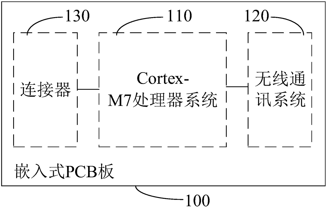
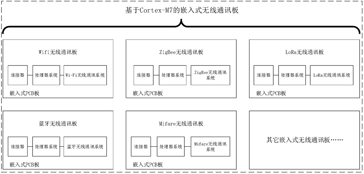
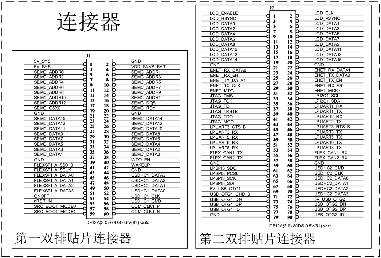
[0037] In order to facilitate the understanding of the present invention, the present invention will be described more fully below with reference to the relevant drawings. The preferred embodiment of the invention is shown in the drawings. However, the present invention can be implemented in many different forms and is not limited to the embodiments described herein. On the contrary, the purpose of providing these embodiments is to make the disclosure of the present invention more thorough and comprehensive.
[0038] It should be noted that when an element is considered to be "connected" to another element, it may be directly connected to and integrated with another element, or there may be a centering element at the same time.
[0039] Unless otherwise defined, all technical and scientific terms used herein have the same meaning as commonly understood by those skilled in the technical field of the present invention. The terminology used in the specification of the present invention herein is only for the purpose of describing specific embodiments, and is not intended to limit the present invention. The term "and/or" as used herein includes any and all combinations of one or more related listed items.
[0040] With the development of the information age, in terms of wireless communication, various original technologies such as Wi-Fi, ZigBee, Bluetooth and Mifare continue to occupy the mainstream position of wireless communication, but newly emerging technologies such as LoRa, NB-IoT (Narrow BandInternet of Things, cellular-based narrowband Internet of Things) and Sigfox are not to be outdone, and continue to impact the position of the original technology.
[0041] The development of wireless communication technology has made more options available, but no matter which wireless communication method is used, it is a major challenge for system designers. There are mainly two traditional design schemes: one is that system designers design the wireless communication circuit by themselves and design it together with other circuits; the other is to use wireless modules that have been designed by other manufacturers, and only need to integrate the wireless modules into Your own design is fine.
[0042] Of the two traditional design schemes: the first is to design the wireless communication circuit by itself, which requires extremely high design capabilities of wireless technology, and the design may fail if you are not careful; the second is to use other manufacturers' designs A good wireless module. In this design, the wireless module needs to occupy a separate area, and due to the antenna, it can only be placed on the edge of the PCB board. There are certain limitations on the layout design, and as long as the wireless module is determined , It is more difficult to replace it, and the design is not flexible enough. Specifically, the wireless module is connected to the bottom plate through a stamp hole package, and the stamp hole forms of the wireless module of different wireless communication methods are different, for example, the number of pins is different, the pin spacing is different, the pin arrangement is different, etc. And so on, this shows that to be reliably connected to the bottom board, a separate area needs to be drawn on the PCB board, and a suitable package pad needs to be designed. At the same time, it is necessary to connect signals according to different interfaces of each module. Once the wireless module in the form of a stamp hole is designed and determined, when the application requires different wireless communication methods, they cannot be directly replaced with each other, and the wireless module or base plate can only be redesigned. In addition, since the wireless module is welded on the bottom plate, the bottom plate will have an important impact on the quality of the wireless signal. If the wireless module is not close to the edge of the board (especially the antenna part), it will seriously affect the antenna signal and affect data transmission. Traditional wireless modules have problems with layout limitations and flexibility.
[0043] To solve the problems of layout limitations and flexibility of traditional wireless modules, in one embodiment, an embedded wireless communication board is provided, such as figure 1 As shown, figure 1 Is a first schematic structural diagram of an embedded wireless communication board in an embodiment, and includes an embedded PCB board 100 of a preset size;
[0044] The embedded PCB board 100 includes a Cortex-M7 processor system 110, a wireless communication system 120 and a connector 130 connected to the Cortex-M7 processor system 110;
[0045] The Cortex-M7 processor system 110 will convert the device signal obtained by converting the communication signal transmitted by the wireless communication system 120 to the peripheral device circuit through the connector 130; the Cortex-M7 processor system 110 will convert the device signal obtained by converting the device signal transmitted by the peripheral device circuit The communication signal is transmitted to the communication device through the wireless communication system 120.
[0046] Specifically, the embedded PCB board 100 with a preset size includes a Cortex-M7 processor system 110, a wireless communication system 120 and a connector 130; the Cortex-M7 processor system 110 is respectively connected to the wireless communication system 120 and the connector 130.
[0047] The wireless communication system 120 can transmit the communication signal to the Cortex-M7 processor system 110. The Cortex-M7 processor system 110 converts the communication signal into a device signal, and transmits the device signal to the peripheral device circuit through the connector 130; The device signal generated by the peripheral device can be transmitted to the Cortex-M7 processor system 110 through the connector 130. The Cortex-M7 processor system 110 converts the device signal into a communication signal, and transmits the communication signal to the communication device through the wireless communication system 120 .
[0048] It should be noted that in the traditional technology, the wireless modules of different wireless communication methods have different sizes, and the problem of size incompatibility is likely to occur when the wireless module is replaced; in the embodiment of the present invention, the preset size is used for a unified embedded wireless communication board The size of the embedded wireless communication board is not compatible when the device is replaced with a wireless communication method.
[0049] The wireless communication system only includes one wireless communication method; the embedded wireless communication board can select the corresponding wireless communication system according to actual needs to form a series of embedded wireless communication boards with preset sizes and different wireless communication methods.
[0050] The connector includes a variety of pin resources, which can be used to connect the embedded wireless communication board and the peripheral device circuit, which is convenient for the device to quickly replace the embedded wireless communication board without redesigning.
[0051] In traditional technology, wireless modules of different communication modes have different sizes and pins, and cannot be directly replaced; in the embodiment of the present invention, the size of the embedded PCB board can be set according to requirements, forming a series of embeddings with the same size and different communication modes. Type wireless communication board; the device installed with the embedded wireless communication board can select the embedded wireless communication board of the corresponding wireless communication mode when the wireless communication method needs to be replaced, and directly embed and replace it without redesigning the device bottom plate , To solve the limitation of wireless communication in the layout and use flexibility.
[0052] According to the requirements of the wireless communication mode, the Cortex-M7 processor system can be integrated with different wireless communication systems in the embodiments of the present invention, and the remaining resources of the processor system are led out through the connector to form a series of size and pin-compatible embedded wireless Communication board: When the device needs different wireless communication methods, it can quickly replace the embedded wireless communication board without redesigning, solving the problem of wireless communication layout limitations and improving design flexibility.
[0053] The embedded wireless communication board of the embodiment of the present invention can be applied to the Internet of Things, man-machine interface, motor control, etc. The structural dimensions, connector specifications and pin signal definitions of a series of embedded wireless communication boards are fully compatible. By replacing the embedded wireless communication board installed on the device application baseboard, different wireless communication functions can be realized, which greatly improves the system. Design flexibility.
[0054] In one embodiment, such as figure 2 As shown, figure 2 It is a schematic structural diagram of different communication methods of the embedded wireless communication board in an embodiment. The wireless communication system is a Wi-Fi wireless communication system, a ZigBee wireless communication system, a LoRa wireless communication system, a Bluetooth wireless communication system, or a Mifare wireless communication system.
[0055] Specifically, the wireless communication system can be Wi-Fi wireless communication system, ZigBee wireless communication system, LoRa wireless communication system, Bluetooth wireless communication system or Mifare wireless communication system; the communication method of the embedded wireless communication board can be Wi-Fi, ZigBee, LoRa, Bluetooth or Mifare.
[0056] It should be noted that an embedded wireless communication board contains only one wireless communication method. For example, a Wi-Fi wireless communication board (belonging to an embedded wireless communication board) has only Wi-Fi wireless communication functions, and a ZigBee wireless communication board ( An embedded wireless communication board) has only ZigBee wireless communication function, a LoRa wireless communication board (belonging to an embedded wireless communication board) has only LoRa wireless communication function, and so on.
[0057] In one embodiment, the wireless communication system includes a wireless chip or wireless module connected to the Cortex-M7 processor system;
[0058] The wireless communication system also includes amplifiers, filters, matching circuits and antenna RF connectors;
[0059] Amplifier, filter, matching circuit and antenna RF connector are connected to the wireless chip; or,
[0060] The amplifier, filter, matching circuit and antenna RF connector are connected to the wireless module.
[0061] Specifically, the wireless communication system includes a wireless chip or a wireless module, and also includes an amplifier, a filter, a matching circuit, and an antenna RF connector; the Cortex-M7 processor system is connected to the amplifier, filter, matching circuit, and antenna through the wireless chip. RF connector, or connect the amplifier, filter, matching circuit and antenna RF connector separately through the wireless module.
[0062] It should be noted that wireless chips or wireless modules can be used for signal processing; amplifiers and filters can be used for signal adjustment; matching circuits and antenna RF connectors can be used for connecting antennas. The wireless communication system only needs to connect an external suitable antenna.
[0063] In one embodiment, such as image 3 As shown, image 3 It is a schematic diagram of the connector structure of the embedded wireless communication board in an embodiment. The connector includes a first double-row patch connector and a second double-row patch connector connected to the Cortex-M7 processor system.
[0064] Specifically, the embedded wireless communication board can include a first double-row patch connector and a second double-row patch connector; the Cortex-M7 processor system can pass the first double-row patch connector and/or the second The dual-row patch connector leads to resources, which can realize the interaction between peripheral devices and the embedded wireless communication board.
[0065] It should be noted that the specifications and pin signal definitions of the first double-row patch connector and the second double-row patch connector of the same series of embedded wireless communication boards are fully compatible with embedded wireless communication boards with different communication methods Can replace each other.
[0066] In one embodiment, such as image 3 As shown, the first double-row patch connector is a connector including external bus pins, SPI pins, SDIO pins, and reset pins;
[0067] The second double-row patch connector is a connector including LCD pins, Ethernet pins, ADC pins, I2C pins, UART pins, CAN pins, SPI pins, SDIO pins, and USB pins.
[0068] Specifically, the first dual-row patch connector can include external bus pins, SPI pins, SDIO pins, and reset pins; the second dual-row patch connector can include LCD pins, Ethernet pins, etc. , ADC pins, I2C pins, UART pins, CAN pins, SPI pins, SDIO pins, USB pins, etc.
[0069] It should be noted that most of the pin resources of the embedded wireless communication boards of different communication methods are the same, only the part occupied in the wireless communication system is slightly different. For example, Wi-Fi uses SPI and GPIO resources, ZigBee It uses UART and GPIO resources, SPI and GPIO resources used by Mifare, etc. The connector includes a variety of pins, which can ensure that the embedded wireless communication board can be quickly replaced when the device requires different wireless communication methods. No need to redesign; neither need to worry about the design of the wireless communication system, nor need to consider the size and layout of different embedded wireless communication boards, which improves the flexibility of equipment system design and reduces the overall cost of equipment system design.
[0070] In one embodiment, such as image 3 As shown, the first double-row patch connector is a 60-pin connector; the second double-row patch connector is an 80-pin connector.
[0071] Specifically, the first dual-row patch connector can be 60pin, which contains resources such as external bus, SPI, SDIO, and reset; the second dual-row patch connector is 80pin, which contains LCD, Ethernet, ADC , I2C, UART, CAN, SPI, SDIO and USB and other resources. The specific pin arrangement definition of the connector can be as image 3 Shown.
[0072] In one embodiment, the connector (including the first dual-row patch connector and the second dual-row patch connector) has a pin pitch of 0.5mm (millimeters), a height of 2.2mm, and can be installed in the embedded The bottom surface of the embedded PCB board; in addition to the pin resources used by the devices on the embedded PCB board, other resources can be led out through the double-row patch connector on the bottom surface.
[0073] In one embodiment, such as Figure 4 As shown, Figure 4 As the second schematic structural diagram of the embedded wireless communication board in an embodiment, the Cortex-M7 processor system includes Cortex-M7 processors connected to the wireless communication system and connectors, and memory connected to the Cortex-M7 processor. Power supply circuit, reset circuit, data memory and program memory.
[0074] Specifically, the Cortex-M7 processor system may include Cortex-M7 processor, memory, power circuit, reset circuit, data memory, and program memory; Cortex-M7 processor is connected to memory, power circuit, reset circuit, data memory, and Program memory.
[0075] It should be noted that the Cortex-M7 processor can be the NXP i.MXRT1050 series processor of Cortex-M7; the reset circuit can include a watchdog.
[0076] In one embodiment, such as Figure 5 As shown, Figure 5 Is a schematic diagram of the structure of the embedded PCB board of the embedded wireless communication board in an embodiment, the preset size includes a length size and a width size;
[0077] The value range of the length dimension is 46-50 mm;
[0078] The range of the width dimension is 28 to 32 mm.
[0079] Specifically, the size of the embedded PCB board can be: the length is between 46 to 50 mm, and the width is between 28 to 32 mm; according to actual needs, a series of embedded wireless communications with fixed dimensions and different communication methods can be prepared. board.
[0080] In one embodiment, such as Figure 5 As shown, the embedded PCB board is a rectangular PCB board with fixed round holes and notches;
[0081] The length dimension is 48 mm;
[0082] The width dimension is 30 mm;
[0083] The number of fixed round holes is 2, 3 or 4; the diameter of the fixed round holes ranges from 2 to 2.2 mm, or 2.2 to 2.4 mm;
[0084] The gap is a semi-circular arc gap.
[0085] Specifically, the size of the embedded PCB board can be 48mm (millimeters) * 30mm, with fixed round holes and notches; the number of fixed round holes is at least two, and the diameter of the fixed round holes is 2 to 2.2 mm, or , 2.2 to 2.4 mm.
[0086] Specifically, the lower left corner and upper right corner of the embedded PCB board are each provided with a fixed circular hole with a diameter of 2.2mm, and a semi-circular arc notch is provided directly above to indicate the installation direction of the embedded wireless communication board. The triangle mark is used to indicate the first pin position of the connector.
[0087] On the other hand, the embodiment of the present invention also provides an embedded wireless communication device, such as Image 6 As shown, Image 6 Is a schematic structural diagram of an embedded wireless communication device in an embodiment, including a device backplane;
[0088] The device backplane includes the embedded wireless communication board as described above, and the peripheral connector, peripheral device circuit and antenna connected to the embedded wireless communication board.
[0089] Specifically, the embedded wireless communication device includes a device backplane, which includes an embedded wireless communication board, a peripheral connector, a peripheral device circuit, and an antenna; the embedded wireless communication board is connected to the peripheral connector, the peripheral device circuit, and the antenna, respectively.
[0090] The embodiment of the present invention combines the Cortex-M7 processor system with various wireless communication systems to form a series of fully compatible embedded wireless communication boards with structural dimensions, connector specifications and pin signal definitions; The patch connector is led out, and the antenna is led out through the RF connector of the IPEX interface; by changing different embedded wireless communication boards and connecting them by the connector, the embedded wireless communication device can realize different wireless communication methods, which greatly improves the device system design The flexibility to solve the limitation of equipment in wireless system design.
[0091] The embedded PCB board of the embodiment of the present invention includes a Cortex-M7 processor system and a wireless communication system and a connector connected to the Cortex-M7 processor system; the Cortex-M7 processor system converts the communication signal transmitted by the wireless communication system to obtain equipment The signal is transmitted to the peripheral device circuit through the connector; the Cortex-M7 processor system converts the communication signal obtained from the device signal transmitted by the peripheral device circuit and transmits it to the communication device through the wireless communication system. Among them, a wireless communication system includes only one wireless communication method, and the connector includes multiple pin resources. According to the needs of wireless communication methods, the Cortex-M7 processor system can be integrated with different wireless communication systems, and resources are drawn through connectors to ensure that the device can quickly replace the embedded wireless communication board when different wireless communication methods are required. No need to redesign, solve the limitation of wireless communication layout, and improve design flexibility.
[0092] The technical features of the above-mentioned embodiments can be combined arbitrarily. In order to make the description concise, all possible combinations of the various technical features in the above-mentioned embodiments are not described. However, as long as there is no contradiction in the combination of these technical features, All should be considered as the scope of this specification.
[0093] The above-mentioned embodiments only express several embodiments of the present invention, and the descriptions are more specific and detailed, but they should not be understood as limiting the scope of the invention patent. It should be pointed out that for those of ordinary skill in the art, without departing from the concept of the present invention, several modifications and improvements can be made, and these all fall within the protection scope of the present invention. Therefore, the protection scope of the patent of the present invention should be subject to the appended claims.
PUM


Description & Claims & Application Information
We can also present the details of the Description, Claims and Application information to help users get a comprehensive understanding of the technical details of the patent, such as background art, summary of invention, brief description of drawings, description of embodiments, and other original content. On the other hand, users can also determine the specific scope of protection of the technology through the list of claims; as well as understand the changes in the life cycle of the technology with the presentation of the patent timeline. Login to view more.
Similar technology patents
Data processing method and equipment based on blockchain
Owner:ADVANCED NEW TECH CO LTD
Method and device for controlling control operation
Owner:XIAOMI INC
Security policy setting and determining method, and method and device for executing operation by application program
Owner:CHINA MOBILE COMM CO LTD
Method and device for adding video effect, terminal device and storage medium
Owner:BEIJING BYTEDANCE NETWORK TECH CO LTD
Power flow control system
Owner:WUHAN UNIV OF TECH
Classification and recommendation of technical efficacy words
- increase flexibility
Front illuminated back side contact thin wafer detectors
Owner:OSI OPTOELECTRONICS
Security guarantee method and system for Windows terminals based on auto white list
Owner:SHENZHEN Y& D ELECTRONICS CO LTD
Precise positionable and compensable heavy-load mechanical arm
Owner:CHONGQING JIAOTONG UNIVERSITY
Method, a system and a device for converting speech
Owner:DICTA DIRECT LLC