Touch display panel and manufacturing method thereof

A touch display panel, panel technology, applied in semiconductor/solid-state device manufacturing, instruments, electrical digital data processing, etc., can solve problems such as increased cost and process risk, and achieve the effect of small process risk and cost reduction

Active Publication Date: 2018-08-24
WUHAN CHINA STAR OPTOELECTRONICS TECH CO LTD
View PDF4 Cites 3 Cited by
  • Summary
  • Abstract
  • Description
  • Claims
  • Application Information

AI Technical Summary

Problems solved by technology

The production of the touch line wiring can be designed separately, that is, the touch line wiring is set separately; the data line mask can also be used, that is, it is set on the same layer as the data line or formed by the same process, and is produced simultaneously with the same metal way, but both solutions have the problem of increased cost and process risk

Method used


Image

  • Touch display panel and manufacturing method thereof
  • Touch display panel and manufacturing method thereof
  • Touch display panel and manufacturing method thereof

Examples


Embodiment Construction

[0011] The following will clearly and completely describe the technical solutions in the embodiments of the present invention with reference to the accompanying drawings in the embodiments of the present invention. Obviously, the described embodiments are only some, not all, embodiments of the present invention. Based on the embodiments of the present invention, all other embodiments obtained by persons of ordinary skill in the art without making creative efforts belong to the protection scope of the present invention.

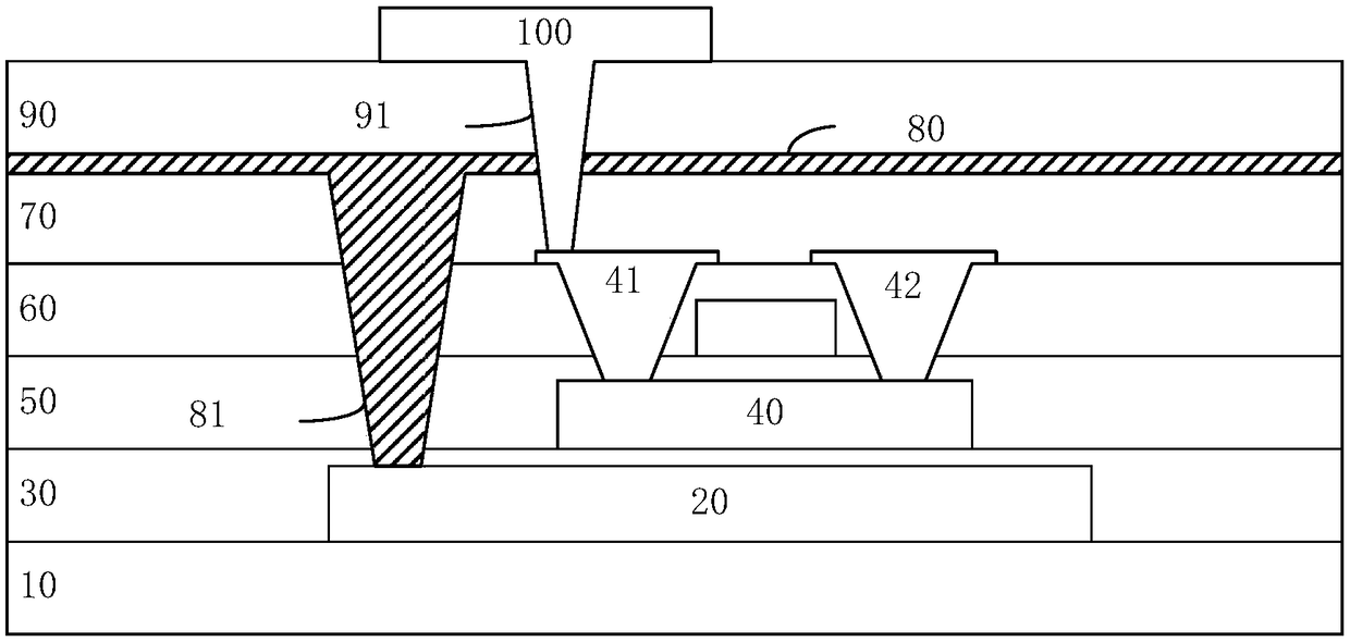
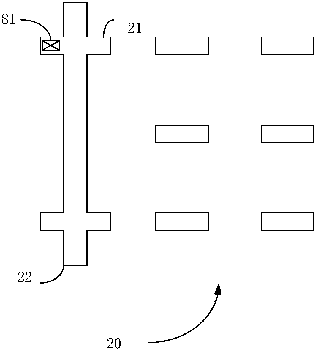
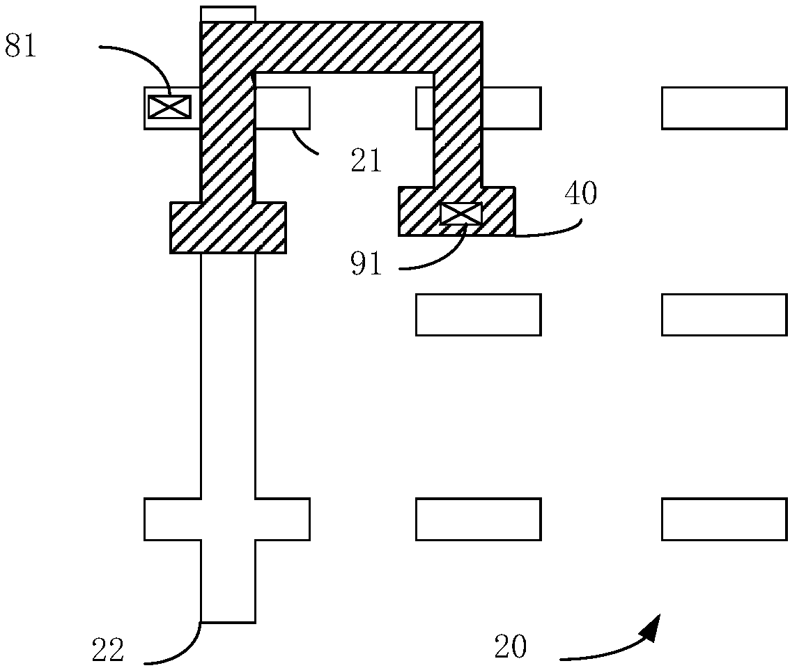
[0012] see figure 1 , figure 1 It is a schematic cross-sectional view of the second embodiment of the touch display panel provided by the present invention. The touch display panel includes a substrate 10, a first metal layer 20, a buffer layer 30, a gate insulating layer 50, an interlayer insulating layer 60, a planarization layer 70, a common electrode layer 80, a passivation layer 90, a pixel electrode layer 100 and a drain electrode electrode 41 and sour...


PUM


Abstract

The invention discloses a touch display panel and a manufacturing method thereof. The touch display panel comprises a substrate, a first metal layer, a TFT functional layer, and a common electrode layer, wherein the first metal layer comprises a touch line and light shielding blocks arranged on the substrate; the TFT functional layer is positioned on the first metal layer, and a first via hole isformed in the TFT functional layer; and the common electrode layer is positioned on the TFT functional layer and connected with the first via hole through the touch line. By virtue of the mode, the manufacturing cost can be lowered and the processing reliability can be improved.

Description

technical field [0001] The invention relates to the field of display panels, in particular to a touch display panel and a manufacturing method thereof. Background technique [0002] The touch type of the LTPS (Low Temperature Poly-silicon, low temperature polysilicon technology) display panel often adopts the self-inductance capacitive type, and the ITP (In Cell Touch Panel, embedded touch screen) is realized by integrating the sensor pad on the array substrate to improve the product quality. quality and value. The structure of the Sensor pad generally includes Common ITO and touch wire routing. The production of the touch line wiring can be designed separately, that is, the touch line wiring is set separately; the data line mask can also be used, that is, it is set on the same layer as the data line or formed by the same process, and is produced simultaneously with the same metal way, but both solutions have the problem of increased cost and process risk. Contents of th...

Claims


Application Information

Patent Timeline
Patent Type & Authority Applications(China)
IPC IPC(8): H01L27/12H01L21/77G06F3/041
CPCG06F3/0412G06F2203/04103H01L27/124H01L27/1259H01L29/78633H01L29/78675
Inventor 聂晓辉
Owner WUHAN CHINA STAR OPTOELECTRONICS TECH CO LTD
Why Eureka
Try Eureka