
Insulator defect detection method, system and terminal equipment

A defect detection and insulator technology, applied in the field of defect detection, can solve problems such as heavy workload, poor safety, and low detection accuracy, and achieve the effects of realizing hidden safety hazards, improving detection accuracy, and improving detection efficiency

Active Publication Date: 2020-09-29
SHENZHEN LAUNCH DIGITAL TECH
View PDF7 Cites 0 Cited by
  • Summary
  • Abstract
  • Description
  • Claims
  • Application Information

AI Technical Summary

Problems solved by technology

[0004] In view of this, the embodiment of the present invention provides an insulator defect detection method, system and terminal equipment to solve the problems of heavy workload, poor safety and low detection accuracy existing in the prior art

Method used


Image

  • Insulator defect detection method, system and terminal equipment
  • Insulator defect detection method, system and terminal equipment
  • Insulator defect detection method, system and terminal equipment

Examples


Embodiment 1

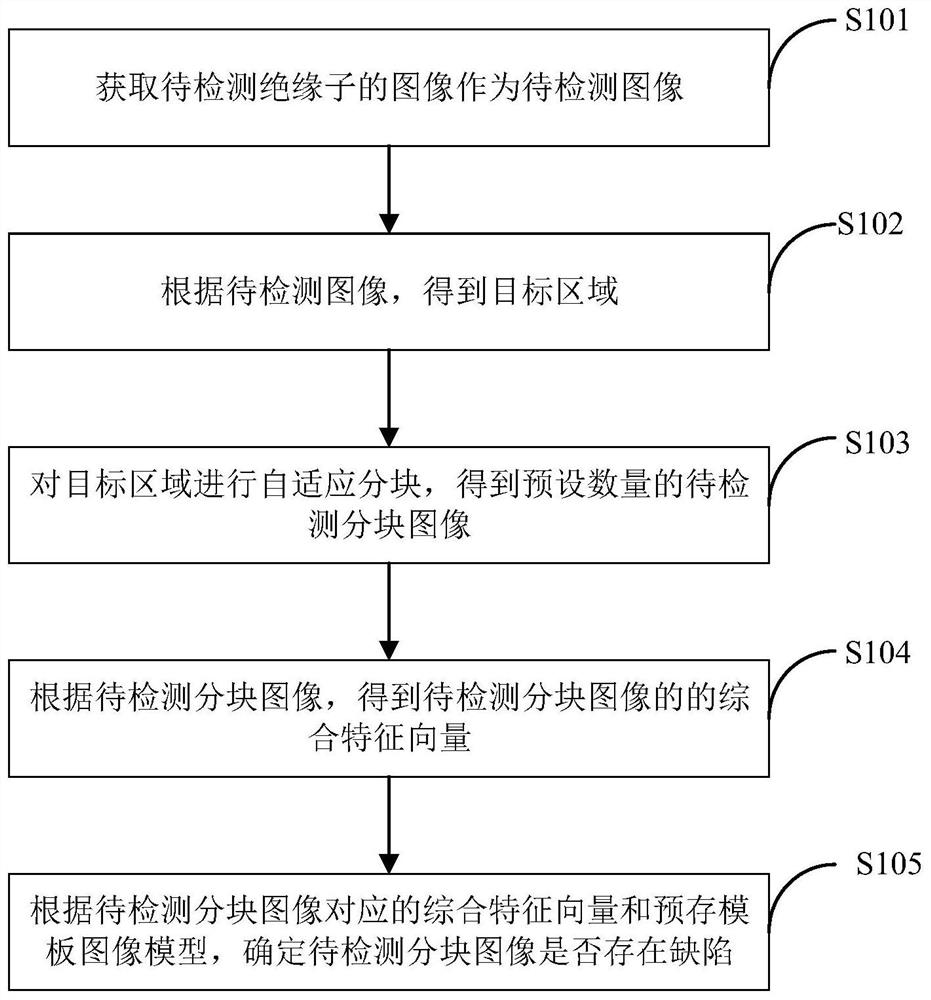
[0033] figure 1 It shows the implementation flow of an insulator defect detection method provided by an embodiment of the present invention, and the process is described in detail as follows:

[0034] In step S101, an image of an insulator to be detected is acquired as an image to be detected.

[0035] In this embodiment, the method of acquiring the image of the insulator to be tested can be taken by a drone, or can be acquired by a fixed camera installed near the insulator to be tested.

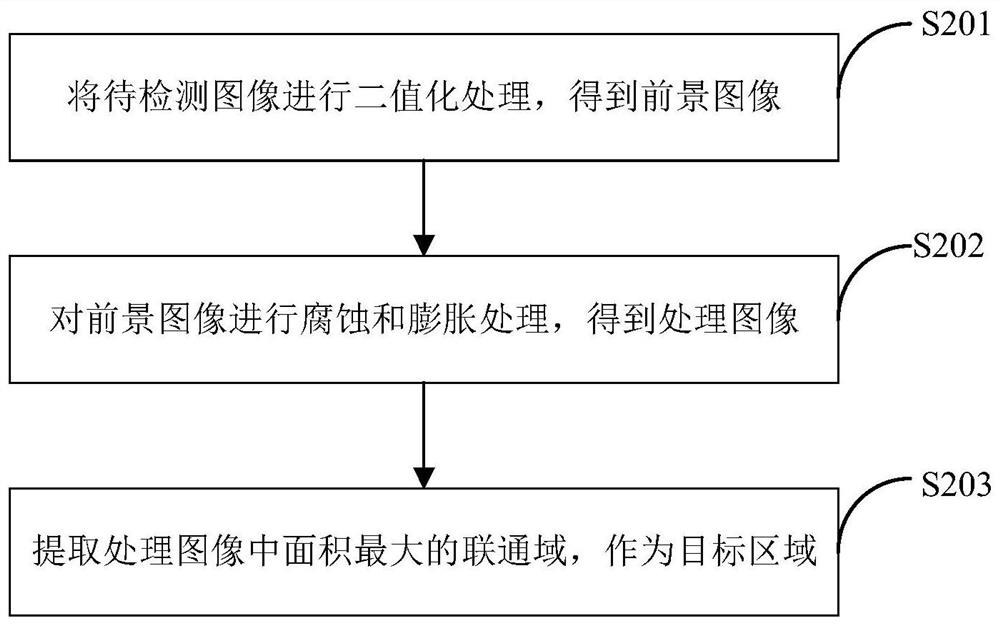
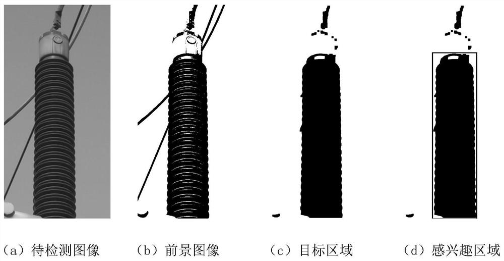
[0036] In step S102, the target area is obtained according to the image to be detected.

[0037] In step S103, the target area is adaptively segmented to obtain a preset number of segmented images to be detected.

[0038] In step S104, according to the block image to be detected, a comprehensive feature vector of the block image to be detected is obtained.

[0039] In step S105, it is determined whether there is a defect in the block image to be detected according to the comprehensive fea...

Embodiment 2

[0108] Such as Figure 5 As shown, an embodiment of the present invention provides an insulator defect detection system 100 for performing figure 1 The method step in the corresponding embodiment, it comprises:

[0109] The image acquisition module 110 to be detected is used to obtain the image of the insulator to be detected as the image to be detected;

[0110] The target area acquisition module 120 is used to obtain the target area according to the image to be detected;

[0111] The segmented image to be detected acquisition module 130 is used for adaptively segmenting the target area to obtain a preset number of segmented images to be detected;

[0112] The integrated feature vector generation module 140 is used to obtain the integrated feature vector of the block image to be detected according to the block image to be detected;

[0113] The defect judging module 150 is configured to determine whether the block image to be detected has defects according to the comprehen...

Embodiment 3

[0147] Such as Figure 8 As shown, the embodiment of the present invention also provides a terminal device 8, including a memory 81, a processor 80, and a computer program 82 stored in the memory 81 and operable on the processor 80, and the processor 80 executes the The computer program 82 realizes the steps in each embodiment as described in Embodiment 1, for example figure 1 Step S101 to step S105 are shown. Alternatively, when the processor 80 executes the computer program 82, it realizes the functions of each module in each device embodiment as described in Embodiment 2, for example Figure 4The functions of modules 110 to 150 are shown.

[0148] The terminal device 8 may be computing devices such as desktop computers, notebooks, palmtop computers, and cloud servers. The terminal device 8 may include, but not limited to, a processor 80 and a memory 81 . For example, the terminal device 8 may also include an input and output device, a network access device, a bus, and t...


PUM


Abstract

The invention is applicable to the technical field of defect detection and provides a method, system and terminal device for detecting defects of an insulator. The method comprises acquiring images ofan insulator to be detected as images to be detected, acquiring a target area according to the images to be detected, carrying out self-adaptive partitioning on the target area to obtain a preset number of block images to be detected, acquiring comprehensive feature vectors of the block images to be detected according to the block images to be detected, and determining whether the block images tobe detected have defects according to the comprehensive feature vectors of the block images to be detected and a pre-stored template image model. The method, system and terminal device realize the automatic detection of the insulator and improve the detection efficiency. Through the comparison between the block images to be detected and the pre-stored template image model, the detection precisionis improved and an effective early warning for the safety hazard of the power device is realized.

Description

technical field [0001] The invention belongs to the technical field of defect detection, and in particular relates to an insulator defect detection method, system and terminal equipment. Background technique [0002] With the production and operation of my country's main 500kV high-voltage transmission lines, the monitoring and maintenance of transmission lines under the new situation has become very urgent and necessary. Among them, the defect detection of insulators, which are used to hold a conductor and insulate it from other conductors, is an important part of transmission line maintenance. During the long-term operation of insulators, due to various reasons, cracks, breaks, and contamination may occur, causing a series of equipment accidents. Therefore, it is necessary to frequently check the appearance of the porcelain bottle of the insulator. [0003] In the prior art, the voltage distribution method or image recognition method based on neural network is usually us...

Claims


Application Information

Patent Timeline
Patent Type & Authority Patents(China)
IPC IPC(8): G01N21/95
CPCG01N21/9515
Inventor 段晶晶李国胜
Owner SHENZHEN LAUNCH DIGITAL TECH
Learn More