A two-chamber double-battery nitrogen oxide sensor chip and its preparation method
A sensor chip, nitrogen oxide technology, applied in instruments, scientific instruments, material analysis by electromagnetic means, etc., can solve the problems of complex circuit design, small size, and difficult production, and achieve simple electronic control units and low production costs. Low and save precious metal material effect
- Summary
- Abstract
- Description
- Claims
- Application Information
AI Technical Summary
Problems solved by technology
Method used
Image
Examples
Embodiment 1
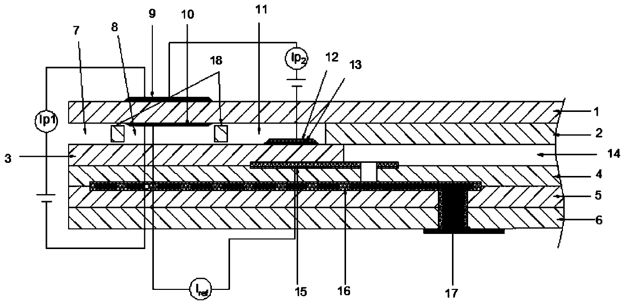
[0032] Such as figure 1 As shown, the first cast substrate layer 1, the third cast substrate layer 3, the fourth cast substrate layer 4 and the fifth cast substrate layer 5 print corresponding functional layers respectively, and the second flow The extended substrate layer 2 and the third cast substrate layer 3 are punched and filled with organic slurry, and the processed six-layer cast substrate is stacked into an integral green body, which is cut and deglued and sintered to form a single nitrogen oxide sensor chip.
[0033] The front side of the first casting substrate layer 1 is printed with a common external electrode 9, the reverse side of the first casting substrate layer 1 is printed with an inactive electrode 10, the front side of the third casting substrate layer 3 is printed with an active electrode 13, and a diffusion barrier is printed on the surface of the active electrode 13. Layer 12, the inactive electrode 10 and the active electrode 13 are separated by the pu...
Embodiment 2
[0041] The novel nitrogen oxide sensor chip and its preparation method in this embodiment, such as image 3 shown. Except the following circumstances, all the other are with embodiment 1:
[0042] The active electrode 13 is printed with platinum-rhodium paste, wherein the platinum content is 97wt%, and the rhodium content is 3wt%.
[0043] Platinum paste for printing the inactive electrode 10, wherein the platinum content of the functional material is 97wt%, and the gold content is 3wt%.
[0044] A common external electrode 9 is printed on the front side of the first casting substrate layer 1 , an inactive electrode 10 and an active electrode 13 are printed on the back side, and a diffusion barrier layer 12 is printed on the surface of the active electrode 13 . The second casting substrate layer 2 is punched to form a first chamber 8 and a second chamber 11 , and the first chamber 8 and the second chamber 11 are connected by a reserved slit diffusion channel 18 .
[0045] T...
PUM
| Property | Measurement | Unit |
|---|---|---|
| electrical resistance | aaaaa | aaaaa |
| viscosity | aaaaa | aaaaa |
| particle diameter | aaaaa | aaaaa |
Abstract
Description
Claims
Application Information


