Pixel arrangement structure, display panel, display device, and mask plate

A pixel arrangement and display panel technology, applied to semiconductor devices, electrical components, circuits, etc., can solve problems such as high difficulty in alignment, color mixing, and small opening size

Active Publication Date: 2018-09-04
BOE TECH GRP CO LTD +1
View PDF6 Cites 8 Cited by
  • Summary
  • Abstract
  • Description
  • Claims
  • Application Information

AI Technical Summary

Problems solved by technology

[0005] Embodiments of the present invention provide a pixel arrangement structure, a display panel, a display device, and a mask, which can solve the problem of high alignment difficulty, color mixing, and low sub-pixel arrangement uniformity caused by the small opening size of the FMM in the prior art. And other issues

Method used


Image

  • Pixel arrangement structure, display panel, display device, and mask plate
  • Pixel arrangement structure, display panel, display device, and mask plate
  • Pixel arrangement structure, display panel, display device, and mask plate

Examples


Embodiment Construction

[0030] The following will clearly and completely describe the technical solutions in the embodiments of the present invention with reference to the accompanying drawings in the embodiments of the present invention. Obviously, the described embodiments are only some, not all, embodiments of the present invention. Based on the embodiments of the present invention, all other embodiments obtained by persons of ordinary skill in the art without making creative efforts belong to the protection scope of the present invention.

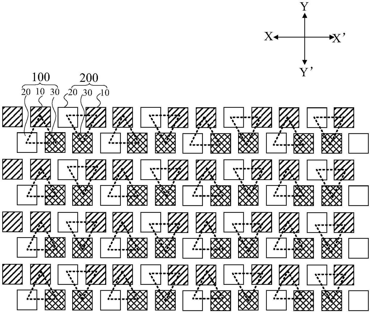
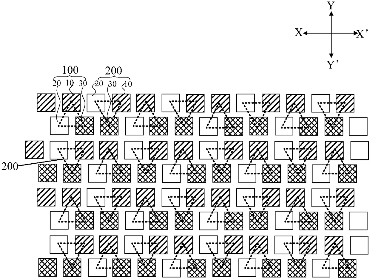
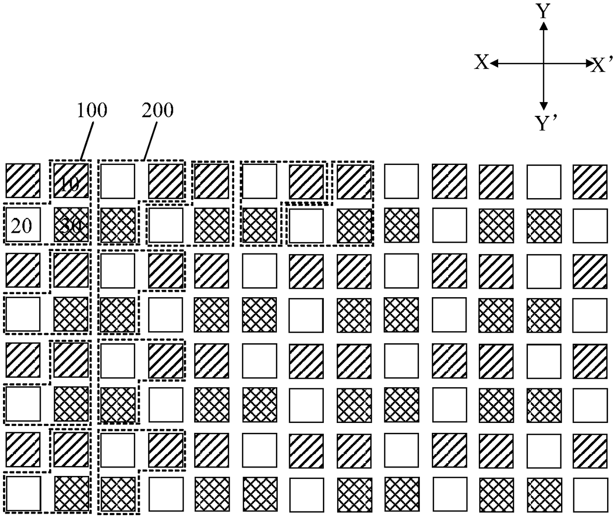
[0031] An embodiment of the present invention provides a pixel arrangement structure, such as figure 1 As shown, the pixel arrangement structure includes a first display unit 100 and a second display unit 200 arranged in an array, wherein the first display unit 100 and the second display unit 200 are arranged alternately along the row direction XX'; A display unit includes three different colors and is distributed in two adjacent rows of the first sub-pixel 10...


PUM


Abstract

The embodiment of the invention, which relates to the field of display technology, provides a pixel arrangement structure, a display panel, a display device, and a mask plate so that problems of highalignment difficulty, color mixing, and low sub-pixel arrangement uniformity caused by the small opening dimension of the FMM in the prior art can be solved. The pixel arrangement structure comprisesfirst display units and second display units, wherein the first display units and the second display units are arranged in an array and are arranged alternately and successively along a row direction.Each display unit consists of a first sub pixel, a second sub pixel, and a third sub pixel that have three kinds of different colors and are distributed at two adjacent rows. For one group of first display units and one group of second display units adjacent to the first display units in a first direction, the first sub pixels in the first display units and the first sub pixels and the second subpixels in the second display units are arranged at the same row; and the second sub pixels and the third sub pixels in the first display units and the third sub pixels in the second display units arearranged at the same row.

Description

technical field [0001] The invention relates to the field of display technology, in particular to a pixel arrangement structure, a display panel, a display device, and a mask. Background technique [0002] With the continuous improvement of display technology, people's requirements for display devices are also constantly increasing. Among various display technologies, high-resolution and high-definition display devices are increasingly used in high-performance display fields. [0003] Among them, during the manufacturing process of the display device, it is generally necessary to use a high-precision metal mask (Fine Metal Mask, FMM) to form some patterned film layers related to sub-pixels through an evaporation process; for example, for Organic Light Emitting Diodes (Organic Light For the Emitting Diode (OLED) display device, in the prior art, FMM is mostly used to manufacture the light emitting pattern layer of the OLED device, wherein the size of the opening in the FMM is...

Claims


Application Information

Patent Timeline
IPC IPC(8): H01L27/32
CPCH10K59/353
Inventor 何潘婷罗昶梅菊
Owner BOE TECH GRP CO LTD
Why Eureka
Try Eureka