
Display panel and display device

A display panel and display area technology, applied in static indicators, instruments, semiconductor devices, etc., can solve the problems affecting the display effect of the display panel, and achieve the effect of improving the display effect, reducing the area, and improving the uniformity of the arrangement.

Active Publication Date: 2021-01-22
KUNSHAN GO VISIONOX OPTO ELECTRONICS CO LTD
View PDF2 Cites 2 Cited by
  • Summary
  • Abstract
  • Description
  • Claims
  • Application Information

AI Technical Summary

Problems solved by technology

[0003] Based on this, it is necessary to provide a display panel and a display device that improve the above-mentioned problems in view of the problem that the different arrangement density of the circuit modules of the demultiplexing circuit affects the display effect of the display panel.

Method used


Image

  • Display panel and display device
  • Display panel and display device

Examples


Embodiment Construction

[0033] In order to make the above objects, features and advantages of the present invention more comprehensible, specific implementations of the present invention will be described in detail below in conjunction with the accompanying drawings. In the following description, numerous specific details are set forth in order to provide a thorough understanding of the present invention. However, the present invention can be implemented in many other ways different from those described here, and those skilled in the art can make similar improvements without departing from the connotation of the present invention, so the present invention is not limited by the specific embodiments disclosed below.

[0034] In describing the present invention, it should be understood that the terms "center", "longitudinal", "transverse", "length", "width", "thickness", "upper", "lower", "front", " Back", "Left", "Right", "Vertical", "Horizontal", "Top", "Bottom", "Inner", "Outer", "Clockwise", "Counte...


PUM


Abstract

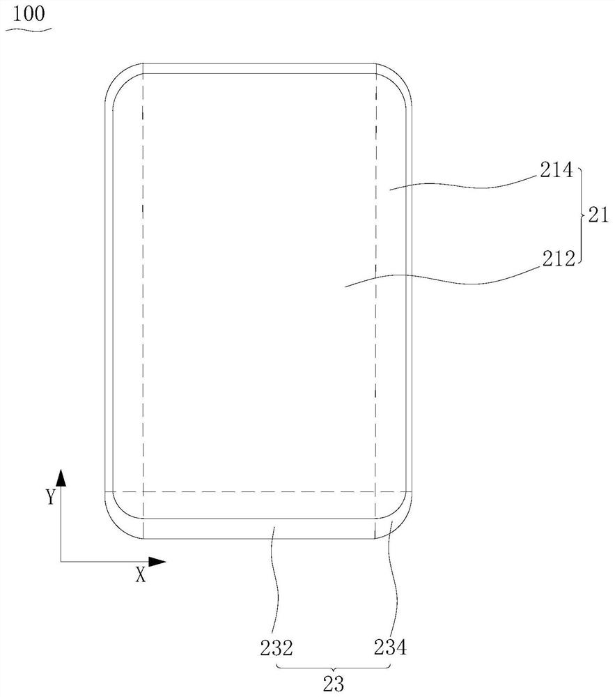
The invention relates to a display panel and a display device. The display panel comprises a substrate; a demultiplexing circuit which is formed in a non-display area of the substrate and comprises aplurality of groups of thin film transistor units which are arranged at intervals along a first direction, wherein each group of thin film transistor units comprises at least one thin film transistor;a plurality of groups of dummy units which are formed in the non-display area of the substrate, wherein each group of dummy units comprises at least one dummy semiconductor monomer, any one group ofdummy units is located between two groups of thin film transistor units which are adjacently arranged in the first direction, and the distance between any one group of thin film transistor units and the other group of thin film transistor units which are most adjacent to the any one group of thin film transistor units is smaller than a preset distance; or the distance between any group of thin film transistor units and the most adjacent dummy unit is less than the preset distance. According to the display panel, the arrangement uniformity of the circuit modules in the non-display area is effectively improved, and TFT characteristic differences caused by different arrangement densities of the thin film transistor units are effectively eliminated.

Description

technical field [0001] The present invention relates to the field of display technology, in particular to a display panel and a display device. Background technique [0002] On electronic devices such as mobile phones and tablet computers, users have higher and higher requirements for the frame width of the display panel. The circuit modules of the sub-circuit are densely arranged in a limited space. The density of the arrangement of the circuit modules is different, resulting in differences in the TFT characteristics (including parameters such as on-state current, off-state current, turn-on voltage, electron mobility, and switch current ratio) of the thin-film transistors in the demultiplexing circuit. Affects the display effect of the display panel. Contents of the invention [0003] Based on this, it is necessary to provide a display panel and a display device which can improve the above-mentioned problem in view of the problem that the different arrangement density o...

Claims


Application Information

Patent Timeline
Patent Type & Authority Applications(China)
IPC IPC(8): H01L27/32H01L27/12G09G3/3225
CPCH01L27/1214G09G3/3225H10K59/12
Inventor 曹培轩杨路路胡思明
Owner KUNSHAN GO VISIONOX OPTO ELECTRONICS CO LTD
Learn More