Laser processing device and laser processing method

A laser processing method and laser processing technology, applied in metal processing, laser welding equipment, metal processing equipment, etc., can solve problems such as slow processing speed

Active Publication Date: 2022-04-01
HITACHI SEIKO LTD
View PDF7 Cites 0 Cited by
  • Summary
  • Abstract
  • Description
  • Claims
  • Application Information

AI Technical Summary

Problems solved by technology

[0005] However, in the former technique, the shutter is moved mechanically, so the processing speed becomes slow, and in the latter technique, even for the same management information, the number of processes differs for each printed board and does not become the same show disadvantages

Method used


Image

  • Laser processing device and laser processing method
  • Laser processing device and laser processing method
  • Laser processing device and laser processing method

Examples


Embodiment Construction

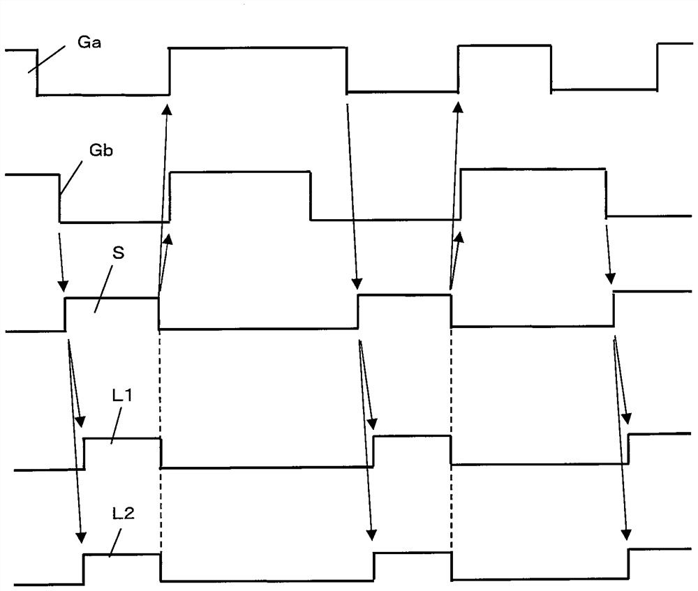
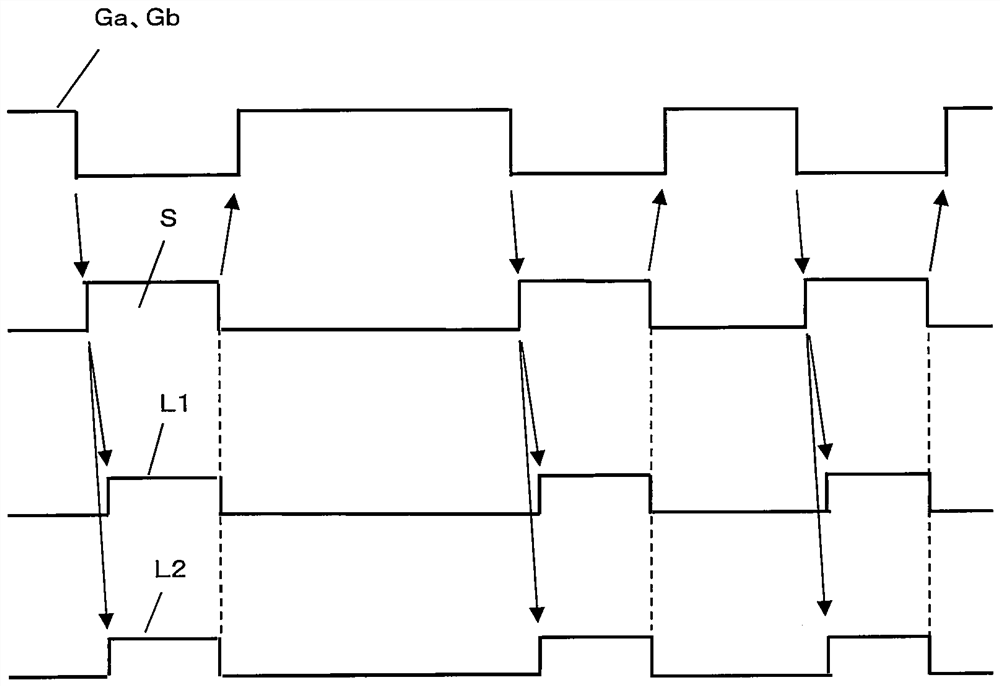
[0022] figure 2 It is a block diagram of a 2-axis type laser processing apparatus which becomes an Example of this invention.

[0023] exist figure 2 Among them, 1a is a laser irradiation unit serving as a first axis, and 1b is a laser irradiation unit serving as a second axis. 2 is a laser oscillator, 3 is a beam splitter (beam splitter) which divides the laser pulse L1 excited by the laser oscillator 2 into two directions, and injects into the laser irradiation unit 1a, 1b respectively. Each of the laser irradiation units 1a and 1b is provided with galvano scanners (galvano scanners) 4a and 4b that move the direction of the received laser pulse L2 two-dimensionally, and fθ that focuses the emitted laser pulses. Lenses 5a, 5b.

[0024] 10a and 10b are printed circuit boards to be processed, and 7 is a table on which the printed circuit boards 10a and 10b are placed. The table 7 can move relative to the laser irradiation units 1a and 1b by moving the table driving unit 8...


PUM


Abstract

The present invention relates to a laser processing device and a laser processing method. The object of the present invention is to distribute laser pulses output from one laser oscillator to a plurality of laser irradiation units and to perform both circuit processing and management processing on a workpiece placed on a table using each laser irradiation unit. Processing using a plurality of laser irradiation units is simultaneously completed without reducing the processing speed and without changing the display of the same management information for each workpiece. A laser processing method that distributes laser pulses from a laser oscillator in a plurality of directions, moves each direction of the distributed laser pulses in a two-dimensional direction, and processes each of a plurality of workpieces for circuits In both the processing for management and processing, the laser processing method is characterized in that the number of processed patterns of the management information recorded in the processing for management is equal to all the management information.

Description

technical field [0001] The present invention relates to a laser processing device and a laser processing method for perforating a workpiece such as a printed circuit board using a laser. Background technique [0002] In a processing device using a laser, it is known that a laser pulse output from one laser oscillator is distributed to a plurality of laser irradiation units, and a printed circuit board placed on a stage is simultaneously processed using each laser irradiation unit to achieve multiple laser beams. A so-called multi-axis laser processing device that speeds up the processing of a printed circuit board. [0003] In such a multi-axis laser processing device, as the processing of printed circuit boards, there are processing of holes for circuits (hereinafter referred to as processing for circuits) and recording of management information represented by characters, symbols, etc. Processing for personal use (hereinafter referred to as processing for management). Reg...

Claims


Application Information

Patent Timeline
Patent Type & Authority Patents(China)
IPC IPC(8): B23K26/00B23K26/0622B23K26/067B23K26/082B23K101/42
CPCB23K26/00B23K26/0622B23K26/0673B23K26/082B23K26/382B23K26/064B23K26/0853B23K2101/42
Inventor 山本雅一二穴胜佐藤征识
Owner HITACHI SEIKO LTD
Why Eureka
Try Eureka