Display panel and display device

A display panel and display area technology, applied in instruments, acquisition/organization of fingerprints/palmprints, optics, etc., can solve problems such as reducing screen-to-body ratio and achieve the effect of increasing screen-to-body ratio

Active Publication Date: 2018-09-07
WUHAN TIANMA MICRO ELECTRONICS CO LTD
View PDF3 Cites 9 Cited by
  • Summary
  • Abstract
  • Description
  • Claims
  • Application Information

AI Technical Summary

Problems solved by technology

[0003] In the existing display devices with fingerprint identification function, the fingerprint identification module is often arranged in the non-display area of ​​the display panel, and the fingerprint identification module is arranged in the non-display area of ​​the display panel, which reduces the screen ratio, and is different from the The development trend of display panel narrowing is contrary to

Method used


Image

  • Display panel and display device
  • Display panel and display device
  • Display panel and display device

Examples


Embodiment Construction

[0023] The present invention will be further described in detail below in conjunction with the accompanying drawings and embodiments. It should be understood that the specific embodiments described here are only used to explain the present invention, but not to limit the present invention. In addition, it should be noted that, for the convenience of description, only some structures related to the present invention are shown in the drawings but not all structures.

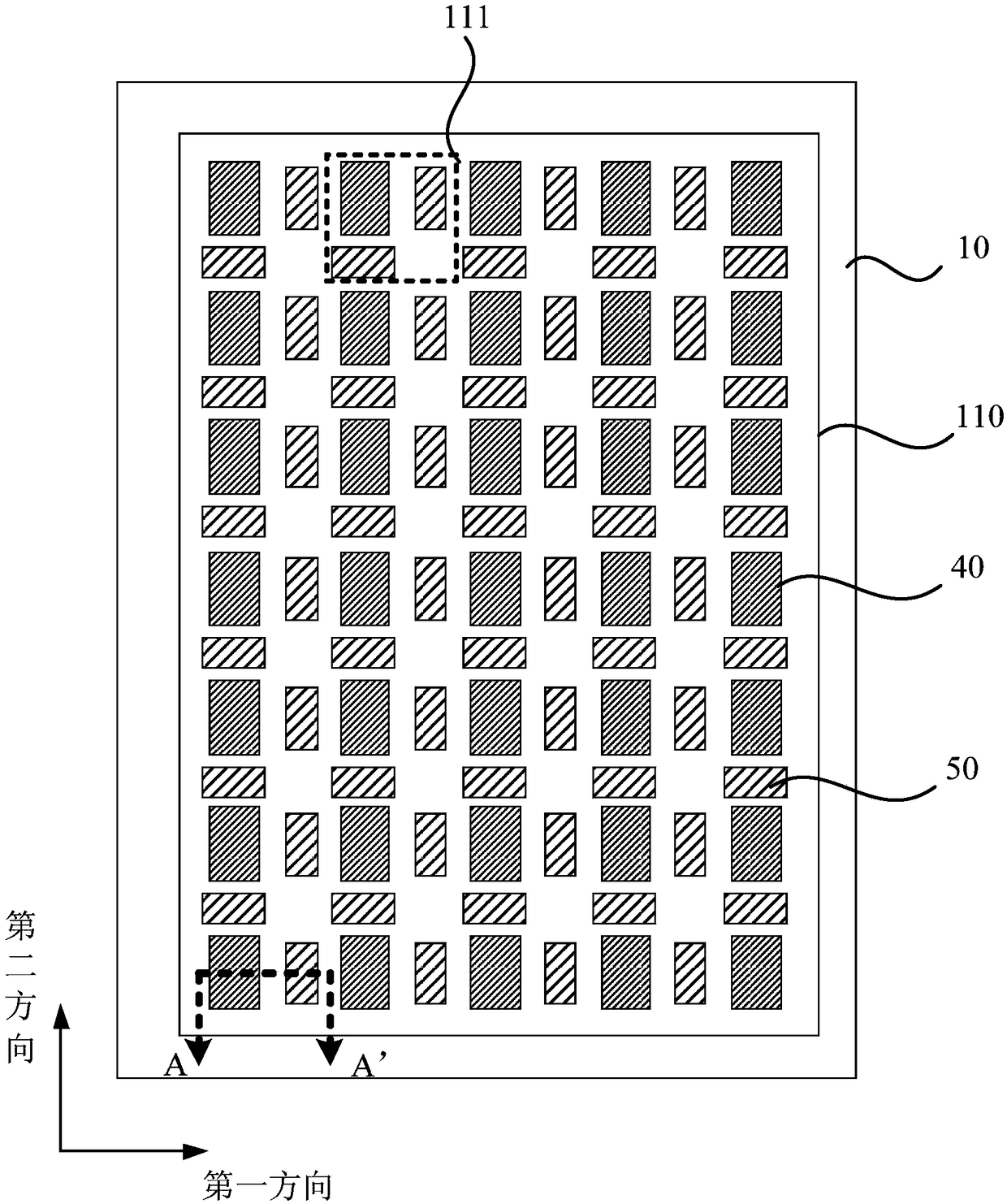
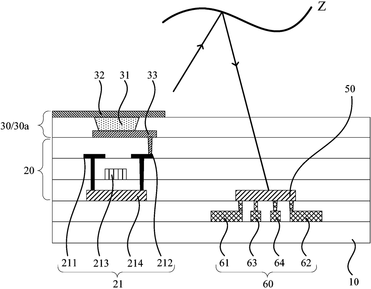
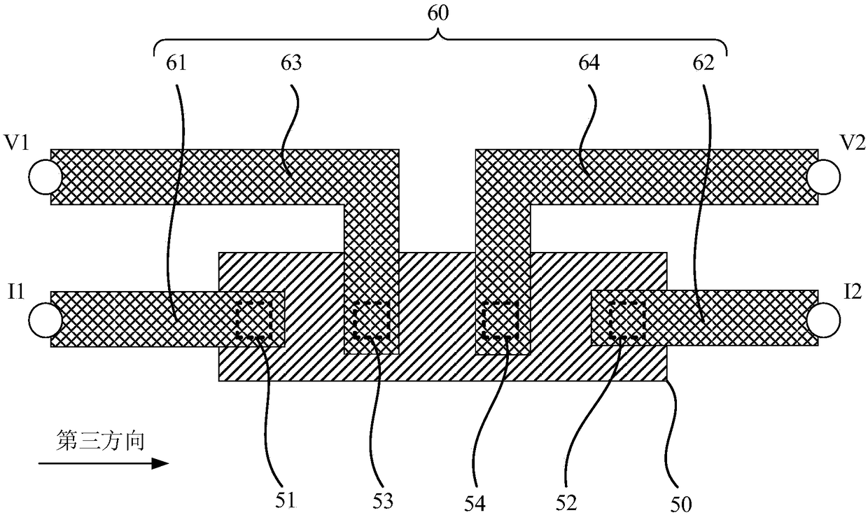
[0024] figure 1 It is a schematic top view structural diagram of a display panel provided by an embodiment of the present invention, figure 2 for along figure 1 A schematic diagram of a cross-sectional structure in the direction of AA', image 3 A schematic diagram of the structure of a semiconductor photosensitive active layer provided in an embodiment of the present invention, refer to figure 1 , figure 2 and image 3 , the display panel includes a display area 110 (the area in the dotted line frame), the...


PUM

PropertyMeasurementUnit
Areaaaaaaaaaaa

Abstract

The invention provides a display panel and a display device. The display panel comprises a display area. The display panel comprises a substrate base plate, a drive circuit layer and a display devicelayer which are laminated. The drive circuit layer is located between the substrate base plate and the display device layer. The display panel also comprises a plurality of pixel units. The pixel units are located in the display area. The display panel also comprises semiconductor photosensitive active layers. Orthographic projections of the semiconductor photosensitive active layers in the planewherein the display panel is are located between the orthographic projections of two adjacent pixel units in the plane wherein the display panel is. The semiconductor photosensitive active layers comprise first signal input ends, second signal input ends, first signal output ends and second signal output ends. The display panel realizes fingerprint identification according to current-voltage characteristics of the semiconductor photosensitive active layers. According to the display panel and the display device provided by the invention, a screen-to-body ratio is improved.

Description

technical field [0001] The present invention relates to the field of display technology, in particular to a display panel and a display device. Background technique [0002] Since fingerprints are inherent to each person, they are unique. With the development of technology, a variety of display devices with fingerprint identification functions and electronic devices including display devices, such as mobile phones, tablet computers, and smart wearable devices, have appeared on the market. In this way, before operating the display device with fingerprint recognition function, the user only needs to touch the fingerprint recognition module of the display device with his finger to perform authority verification, which simplifies the authority verification process. [0003] In the existing display devices with fingerprint identification function, the fingerprint identification module is often arranged in the non-display area of ​​the display panel, and the fingerprint identific...

Claims


Application Information

Patent Timeline
IPC IPC(8): H01L27/32G02F1/1362G06K9/00
CPCG02F1/136286G06V40/1318H10K59/60H10K59/65
Inventor 朱家柱袁山富彭涛周瑞渊
Owner WUHAN TIANMA MICRO ELECTRONICS CO LTD
Why Eureka
Try Eureka