Single wavelength ellipsometry with improved spot size capability

A light beam and light collection technology, applied in the field of metering systems

Active Publication Date: 2018-09-28
KLA CORP
View PDF8 Cites 0 Cited by
  • Summary
  • Abstract
  • Description
  • Claims
  • Application Information

AI Technical Summary

Problems solved by technology

[0011] Future metrology applications present challenges due to small feature sizes and multi-parameter correlations

Method used


Image

  • Single wavelength ellipsometry with improved spot size capability
  • Single wavelength ellipsometry with improved spot size capability
  • Single wavelength ellipsometry with improved spot size capability

Examples


Embodiment Construction

[0032] Reference will now be made in detail to background examples and some embodiments of the invention, examples of which are illustrated in the accompanying drawings.

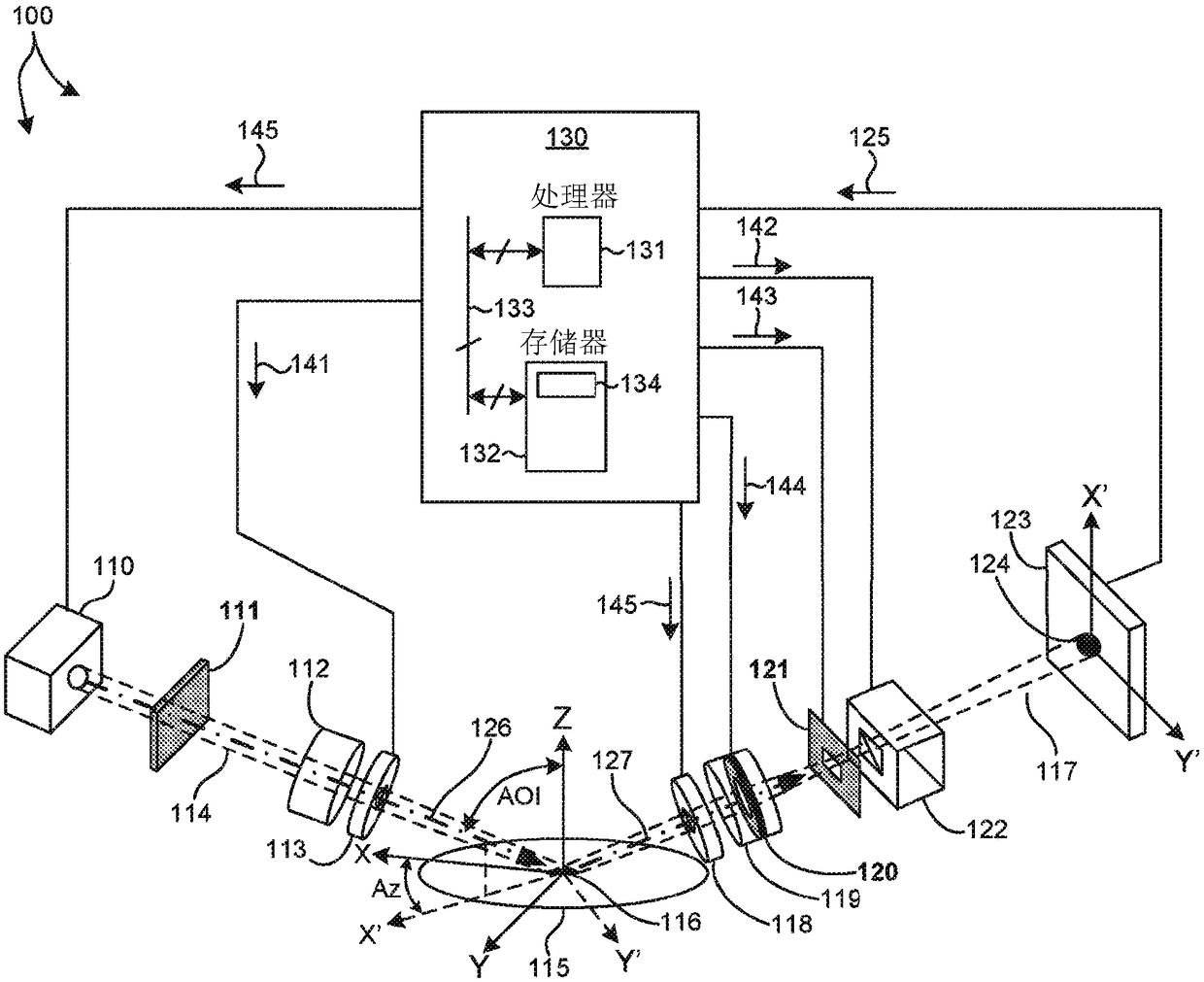
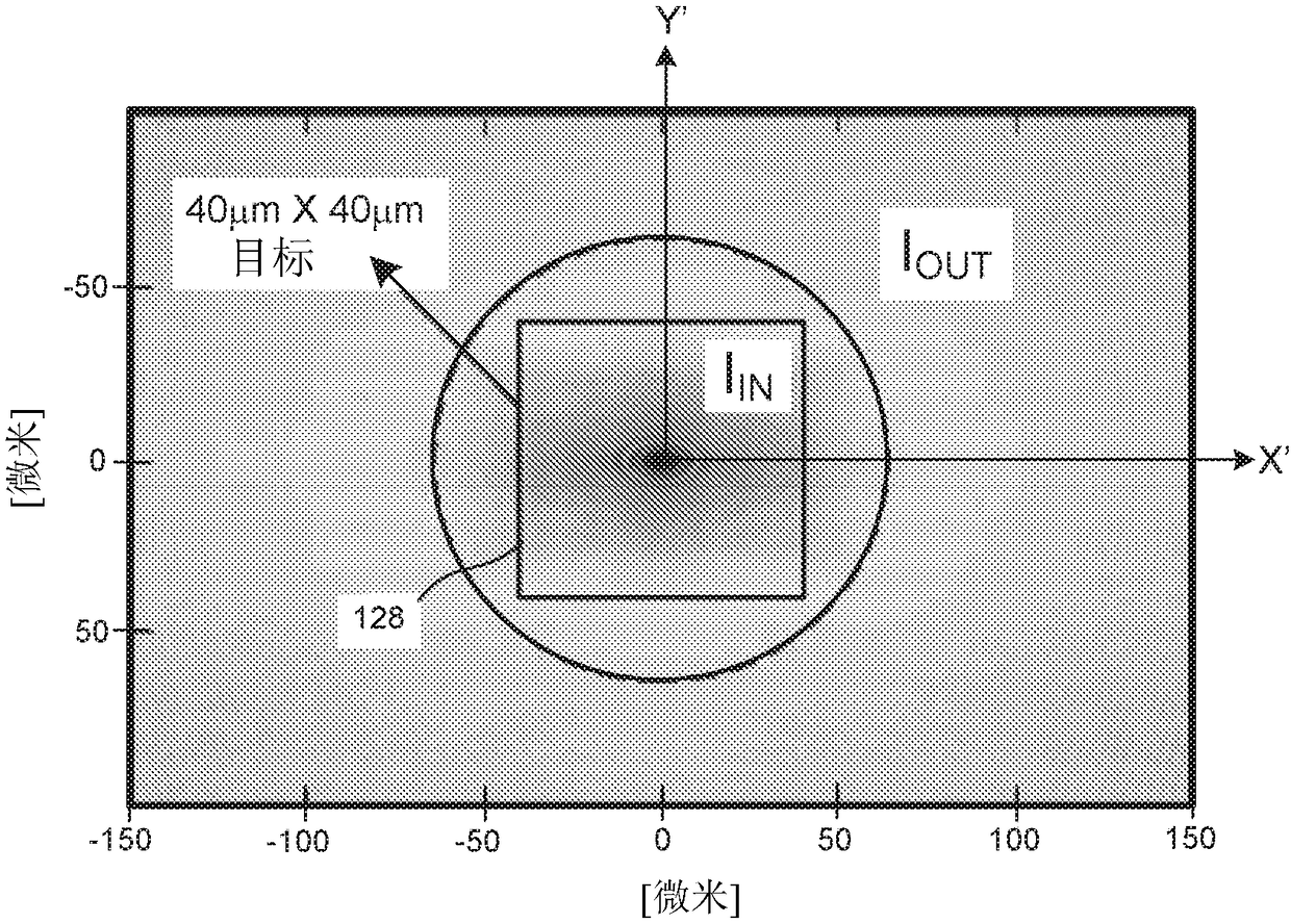
[0033] Presented herein are methods and systems for performing single wavelength ellipsometry (SWE) measurements with reduced measurement spot size. The measurement spot size reduction is achieved by the inclusion of: 1) a pupil stop located in the collection optical path at a position close to the pupil plane of the SWE system; 2) a field stop located close to the SWE In the collection optical path at the location of the image plane conjugate to the wafer plane of the system; 3) a linear polarizer comprising a thin, high extinction ratio, nanoparticle-based polarizer element located in the SWE system in the illumination path between the illumination source and the wafer; or any combination thereof. Reducing the measurement spot size will allow for more accurate thin film measurements and enhanced tool-to-t...


PUM


Abstract

Methods and systems for performing single wavelength ellipsometry (SWE) measurements with reduced measurement spot size are presented herein. In one aspect, a pupil stop is located at or near a pupilplane in the collection optical path to reduce sensitivity to target edge diffraction effects. In another aspect, a field stop is located at or near an image plane conjugate to the wafer plane in thecollection optical path to reduce sensitivity to undesired optical-structural interactions. In another aspect, a linear polarizer acting on the input beam of the SWE system includes a thin, nanoparticle based polarizer element. The nanoparticle based polarizer element improves illumination beam quality and reduces astigmatism on the wafer plane. The pupil and field stops filter out unwanted lightrays before reaching the detector. As a result, measurement spot size is reduced and tool-to-tool matching performance for small measurement targets is greatly enhanced.

Description

[0001] Cross References to Related Applications [0002] This patent application asserts the title of "Methods of Improved Spot Size Capability in Single Wavelength Ellipsometry" filed on January 22, 2016 under 35 U.S.C. §119 Priority to US Provisional Patent Application No. 62 / 286,279, the subject matter of which is hereby incorporated by reference in its entirety. technical field [0003] The embodiments relate to metrology systems and methods, and more particularly, the embodiments relate to methods and systems for improved metrology of semiconductor structures. Background technique [0004] Semiconductor devices, such as logic and memory devices, are typically fabricated through a series of processing steps applied to samples. Various features and multiple structural levels of the semiconductor device are formed through these processing steps. For example, photolithography, among other things, is a semiconductor manufacturing process that involves creating patterns on...

Claims


Application Information

Patent Timeline
Patent Type & Authority Applications(China)
IPC IPC(8): G01N21/21G01N21/95
CPCG01N21/9501G01B2210/56G01B11/065G01N21/211
Inventor E·沙欧辛王福敏K·彼得林茨希佟·郭D·卡瓦门U·格林葆D·R·希尼根
Owner KLA CORP
Why Eureka
Try Eureka