Method and device for processing superblock based on NAND flash

A processing method and data block technology, applied in the field of storage, can solve problems such as the reduction of available storage space of storage devices, and achieve the effects of improving effective utilization, saving storage space, and working efficiently

Inactive Publication Date: 2018-10-02
GIGADEVICE SEMICON (BEIJING) INC
View PDF5 Cites 8 Cited by
  • Summary
  • Abstract
  • Description
  • Claims
  • Application Information

AI Technical Summary

Problems solved by technology

[0004] The embodiment of the present invention provides a NAND flash-based super data block processing method and device to solve the problem in the prior art that the available storage space in the storage device decreases rapidly due to the increase of bad blocks in the super data block

Method used


Image

  • Method and device for processing superblock based on NAND flash
  • Method and device for processing superblock based on NAND flash

Examples


Embodiment 1

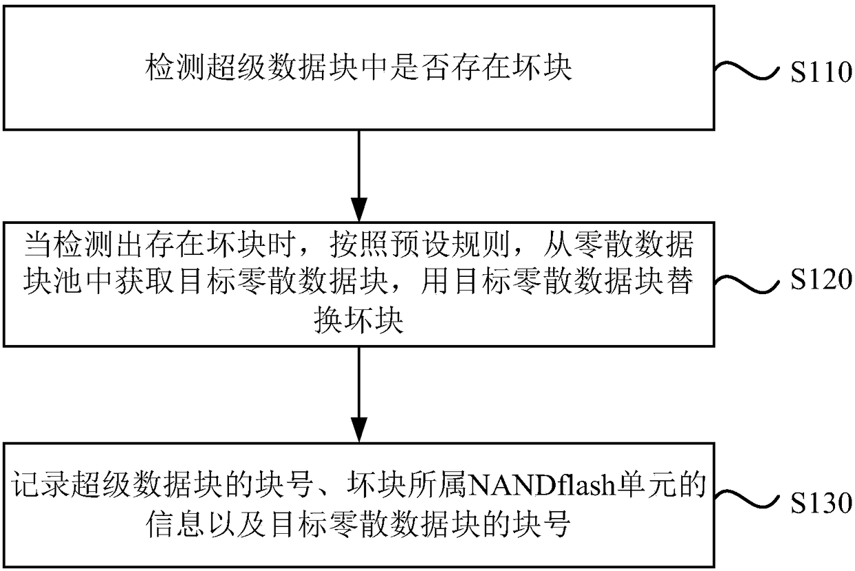
[0020] figure 1 It is a flowchart of a NAND flash-based super block processing method provided by Embodiment 1 of the present invention. This embodiment can be applied to a NAND flash storage device, and the storage device includes at least two NAND flash units. In the storage device It also includes a fragmented data block pool based on the NAND flash unit, including at least one fragmented data block in the fragmented data block pool, the method can be performed by a super data block processing device based on NAND flash, and the device can use software and / or hardware implementation.

[0021] The NAND flash-based super block processing method in Embodiment 1 of the present invention specifically includes:

[0022] S110, detecting whether there is a bad block in the super block;

[0023] NAND flash storage devices read and write data in units of Pages, and erase data in units of Blocks. Each block storage unit is composed of several page storage units. Further, each pag...

Embodiment 2

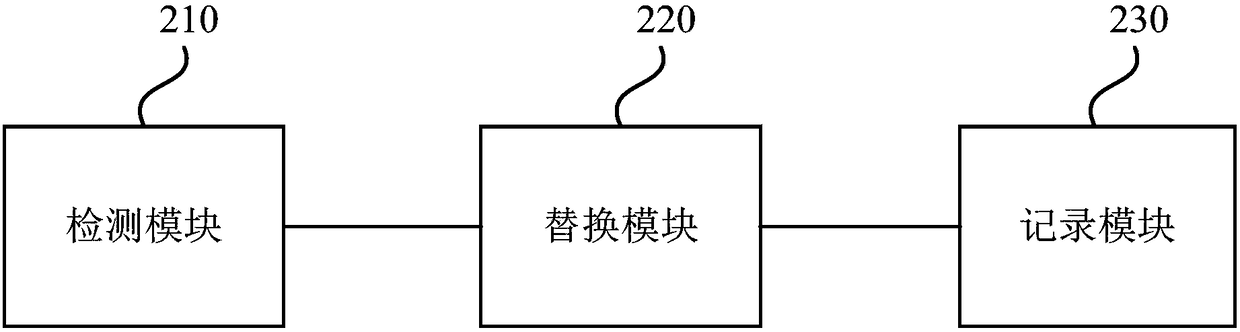
[0034] figure 2 It is a schematic structural diagram of a NAND flash-based super block processing device in Embodiment 2 of the present invention. The device is applied to a NAND flash storage device, and the storage device includes at least two NAND flash units. The storage device also includes a NAND flash-based The fragmented data block pool of the NAND flash unit, the fragmented data block pool includes at least one fragmented data block. Such as figure 2 As shown, the device includes: a detection module 210 , a replacement module 220 and a recording module 230 .

[0035] Wherein, the detection module 210 is used to detect whether there is a bad block in the super block;

[0036] The replacement module 220 is used to obtain the target scattered data block from the scattered data block pool according to preset rules when the detection module 210 detects that there is a bad block in the super block, and replace the bad block with the target scattered data block;

[0037...


PUM


Abstract

Embodiments of the invention disclose a method and a device for processing superblocks based on NAND flash. The method comprises: detecting whether bad blocks exist in the superblocks; when bad blocksare detected, according to a preset rule, obtaining a target sporadic data block from a sporadic data block pool, using the target sporadic data block to replace the bad block; recording the block number of the superblock, information of a NAND flash unit to which the bad block belongs to, and the block number of the target sporadic data block, to manage the replaced superblock. The embodiments solve a problem in the prior art that available storage space is rapidly reduced in a storage device caused by the number of bad blocks in the superblock is increased. Through using the target sporadicdata blocks to replace the bad blocks in the superblock, a new superblock is obtained, excessive bad blocks accumulated in the superblock are prevented, so that storage space is saved, effective utilization of the storage space in the storage device is improved, and the storage device works in higher efficiency.

Description

technical field [0001] The embodiment of the present invention relates to memory technology, and in particular to a NAND flash-based super block processing method and device. Background technique [0002] NAND Flash is a kind of Flash memory and belongs to non-volatile storage device (Non-volatileMemoryDevice). [0003] Usually, for NAND flash-based storage devices, when an uncorrectable read / write / erase error occurs in a data block of the NAND flash, the internal firmware will mark it as a bad block and no longer use it. If multiple NAND flashes are embedded in the storage device, multiple data blocks in the NAND flash form a super data block to be used simultaneously. However, when a certain data block in the super data block is broken, the super data block cannot be used, and as the number of bad blocks increases, the available storage space in the storage device will decrease rapidly. Contents of the invention [0004] Embodiments of the present invention provide a N...

Claims


Application Information

Patent Timeline
Patent Type & Authority Applications(China)
IPC IPC(8): G06F11/10G06F11/20
CPCG06F11/1068G06F11/2017G06F11/2038
Inventor 陈诚
Owner GIGADEVICE SEMICON (BEIJING) INC
Why Eureka
Try Eureka