Detection method and device

A detection method and image technology, applied in image data processing, instruments, calculations, etc., can solve the problems of low identification accuracy of metal balls, inability to effectively detect installation, etc., to improve identification efficiency and accuracy, improve judgment accuracy, and improve detection results. precise effect

Active Publication Date: 2018-10-12
杭州兆图机器人有限公司
View PDF6 Cites 7 Cited by
  • Summary
  • Abstract
  • Description
  • Claims
  • Application Information

AI Technical Summary

Problems solved by technology

[0003] The present invention aims at the problem that the detection equipment in the prior art cannot effectively detect installation defects due to the low recognition accuracy of the metal wires and metal balls after the patch and wire bonding process, and provides a detection method and device, which The technical solution is as follows:

Method used


Image

  • Detection method and device
  • Detection method and device
  • Detection method and device

Examples


Embodiment Construction

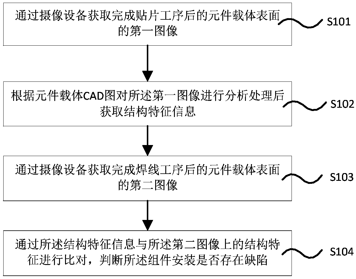
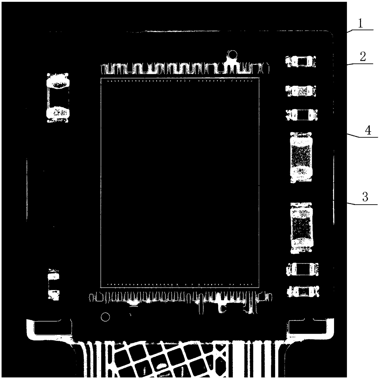
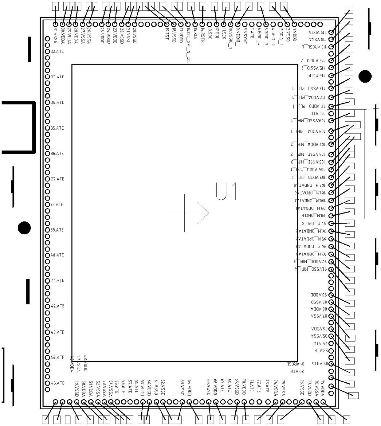
[0026] In order to make the purpose, technical solutions and advantages of the embodiments of the present invention more clear, the following will clearly and completely describe the technical solutions of the embodiments of the present invention in conjunction with the drawings of the embodiments of the present invention. Apparently, the described embodiments are some, not all, embodiments of the present invention. Based on the described embodiments of the present invention, all other embodiments obtained by persons of ordinary skill in the art without creative efforts shall fall within the protection scope of the present invention.

[0027] In the description of the present invention, it should be understood that the terms "first" and "second" are used for description purposes only, and cannot be interpreted as indicating or implying relative importance or implicitly indicating the quantity of indicated technical features. Thus, a feature defined as "first" and "second" may ...


PUM


Abstract

The invention discloses a detection method. By adding an image shooting step after an element carrier sticking working procedure and combining preprocessing information of a computer on a CAD drawing,an image of an element carrier after the sticking working procedure is completed is analyzed, more accurate and practical structure feature information, compared with the CAD drawing, of a tested product is obtained, mounting defects of components such as a metal wire and a metal ball are judged by carrying out comparison on structure features, acquired through analysis on images of element carriers in the same batch after a wire bonding working procedure is finished, by utilizing the structure feature information, defect judgment accuracy is improved, and an error and omission during judgment are avoided.

Description

technical field [0001] The invention relates to the technical field of component defect detection, in particular to a method and a device for detecting installation defects of components mounted on a component carrier. Background technique [0002] An integrated circuit (Integrated Circuit, IC) is a tiny electronic device or component. Using a certain process, the transistors, resistors, capacitors, inductors and other components required in the circuit are interconnected together, and they are fabricated on a small or several small semiconductor chips or dielectric substrates, and then packaged in a tube. It becomes a microstructure with required circuit functions; all the components in it have been formed into a whole structurally, which makes the electronic components take a big step towards miniaturization, low power consumption, intelligence and high reliability. In order to ensure the installation quality of IC components, defect detection for IC components is particu...

Claims


Application Information

Patent Timeline
Patent Type & Authority Applications(China)
IPC IPC(8): G06T7/00
CPCG06T7/0004G06T2207/30141G06T2207/10004
Inventor 赵盾
Owner 杭州兆图机器人有限公司
Why Eureka
Try Eureka