Quasi-nonvolatile memory capable of regulating PN junction based on two-dimensional material and preparation method thereof

A two-dimensional material, non-volatile technology, used in semiconductor devices, electrical solid devices, electrical components, etc., to achieve the effects of simple process, variable structure, and wide applicability

Inactive Publication Date: 2018-10-16
FUDAN UNIV
View PDF4 Cites 5 Cited by
  • Summary
  • Abstract
  • Description
  • Claims
  • Application Information

AI Technical Summary

Problems solved by technology

[0004] Then, compared with traditional silicon-based semi-floating gate transistors, how to design a new type of adjustable quasi-nonvolatile memory by adjusting the energy band structure of two-dimensional materials has become a challenge.

Method used


Image

  • Quasi-nonvolatile memory capable of regulating PN junction based on two-dimensional material and preparation method thereof
  • Quasi-nonvolatile memory capable of regulating PN junction based on two-dimensional material and preparation method thereof
  • Quasi-nonvolatile memory capable of regulating PN junction based on two-dimensional material and preparation method thereof

Examples


Embodiment Construction

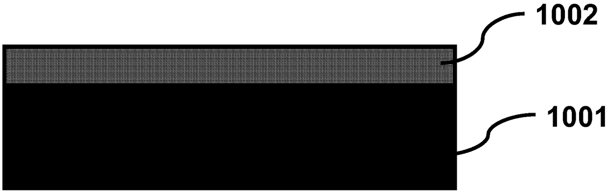
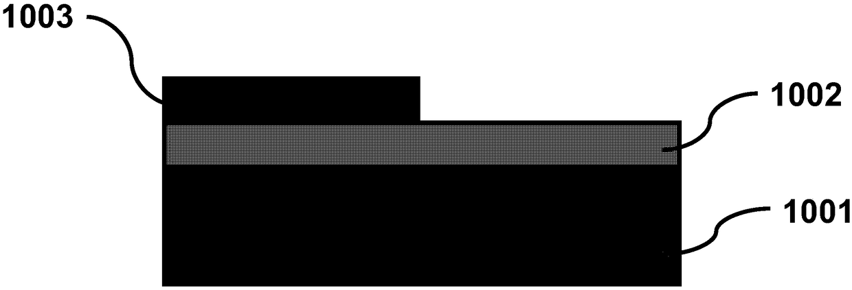
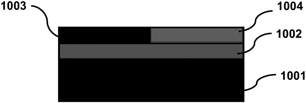
[0046] The above drawings are only some embodiments of the present invention, and those skilled in the art can also obtain other drawings according to these drawings without any creative effort.

[0047] Embodiments of the present invention are described in detail below. Examples of the described embodiments are shown in the drawings, wherein like or similar reference numerals designate like or similar materials or methods having same or similar functions throughout. The embodiments described below by referring to the figures are exemplary only for explaining the present invention and should not be construed as limiting the present invention. To simplify the disclosure of the present invention, the materials and methods of specific examples are described below. Of course, they are only examples and are not intended to limit the invention. In addition, various specific process and material examples are provided herein, but one of ordinary skill in the art will recognize the a...


PUM


Abstract

The invention belongs to the field of micro-nano electronic technology, and is specifically relates to a quasi-nonvolatile memory capable of regulating PN junction based on two-dimensional material and preparation method thereof. The memory comprises a layer of two-dimensional material on the insulating substrate as a charge trapping layer, two other types of two-dimensional materials transferredon the trapping layer, tunneling layer respectively as N region of the PN junction and a flash memory, two-dimensional material stacked on top, and channel layer as P region of the PN junction and a flash memory. According to the quasi-nonvolatile memory capable of regulating PN junction based on two-dimensional material and preparation method thereof, the device can write at the nanosecond leveland the charge retention time is controllable through band designing; By applying a gate voltage to control the turn-on and turn-off of the PN junction, the device can perform ultra-fast writing whenthe PN junction is turned on; By changing the thickness and type of the two materials constituting the PN junction and the ratio of the PN junction area to the insulating layer area, ultra-fast quasi-nonvolatile new memory devices with adjustable retention time can be obtained. The preparation process of the method for the quasi-nonvolatile memory is simple, and the material grown by CVD can be prepared on a large scale.

Description

technical field [0001] The invention belongs to the technical field of micro-nano electronics, and in particular relates to a quasi-nonvolatile memory based on a two-dimensional material adjustable PN junction and a preparation method thereof. Background technique [0002] MOSFET is the most basic unit device in integrated circuits. The progress of technology has made the size of MOSFET transistors shrink and its power density is also increasing; another common device in integrated circuits is floating gate transistors, and floating gate transistors work When writing and erasing at high voltage is required, serious power consumption problems are caused. In order to reduce device power consumption and improve device performance, the concept of semi-floating gate storage technology was first proposed by Fudan University in 2013. The semi-floating gate transistor is a combination of a tunneling field effect transistor and a floating gate device to form a new type of "semi-floa...

Claims


Application Information

Patent Timeline
Patent Type & Authority Applications(China)
IPC IPC(8): H01L27/115
CPCH10B69/00
Inventor 周鹏陈华威张卫
Owner FUDAN UNIV
Why Eureka
Try Eureka