
Post exposure-baking device and optimization method for wafer line width

A post-baking and wafer technology, applied in the field of baking devices, can solve the problems of affecting the lithography line width accuracy, unable to locally heat the hot plate 200, unable to flexibly control the local temperature of the hot plate 200, etc., and achieve high lithography line width accuracy. Effect

Inactive Publication Date: 2018-11-13
SHANGHAI HUALI INTEGRATED CIRCUTE MFG CO LTD
View PDF8 Cites 6 Cited by
  • Summary
  • Abstract
  • Description
  • Claims
  • Application Information

AI Technical Summary

Problems solved by technology

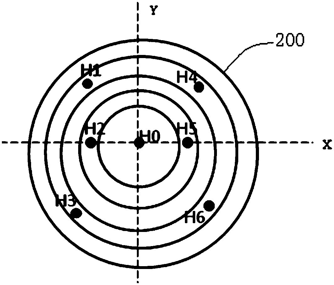
like figure 1 As shown, the hot plate 200 includes seven heating modules (H0 to H6) to heat the hot plate to bake the exposed wafer 100, because the hot plate 200 only includes seven heating modules (H0 to H6), so It is impossible to accurately locally heat the hot plate 200, there are certain heating limitations, and it is impossible to flexibly control the local temperature of the hot plate 200, which affects the accuracy of the lithography line width

Method used


Image

  • Post exposure-baking device and optimization method for wafer line width
  • Post exposure-baking device and optimization method for wafer line width
  • Post exposure-baking device and optimization method for wafer line width

Examples


Embodiment Construction

[0028] The technical solutions in the present invention will be clearly and completely described below in conjunction with the accompanying drawings. Apparently, the described embodiments are part of the embodiments of the present invention, not all of them. Based on the embodiments of the present invention, all other embodiments obtained by persons of ordinary skill in the art without making creative efforts belong to the protection scope of the present invention.

[0029] In the description of the present invention, it should be noted that the orientation or positional relationship indicated by the terms "upward", "downward" and "below" are based on the orientation or positional relationship shown in the drawings, and are only for the convenience of describing the present invention. The invention and the simplified description do not indicate or imply that the device or element referred to must have a specific orientation, be constructed and operate in a specific orientation,...


PUM


Abstract

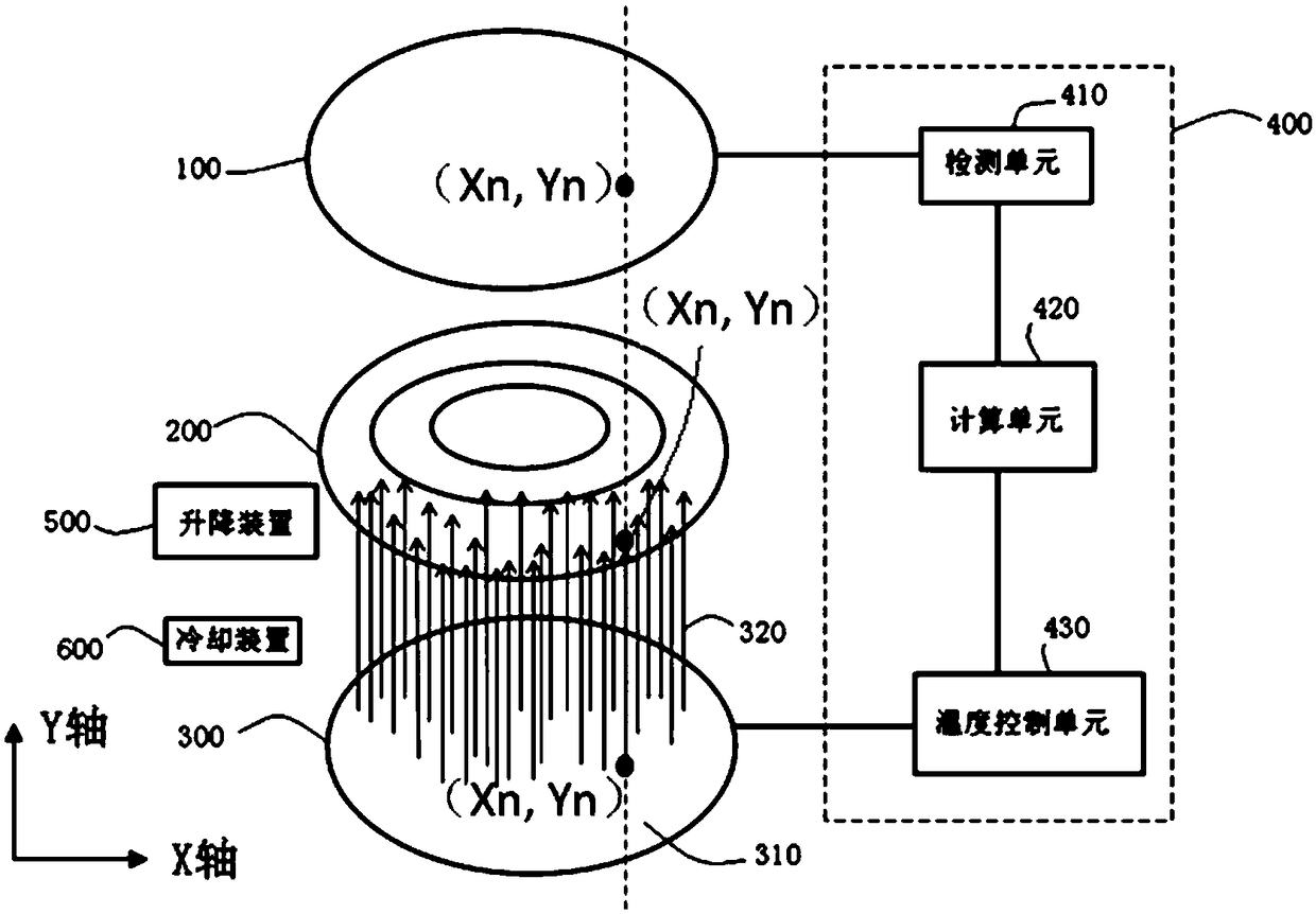
The invention relates to a post exposure-baking device and relates to a manufacturing technology for an integrated circuit. The post exposure-baking device comprises a wafer, a hot plate and a heatingdevice, wherein the hot plate is located below the wafer and is used for heating the wafer; the heating device is located below the hot plate and is used for heating the hot plate; the heating devicecomprises a chassis and a plurality of thermal probes, wherein the plurality of thermal probes are arranged on the chassis and the temperatures of the plurality of the thermal probes are controllable, so that local temperature of the hot plate is adjustable, and further the line width on the wafer is adjusted to achieve higher lithography accuracy of the line width.

Description

technical field [0001] The invention relates to an integrated circuit manufacturing technology, in particular to a baking device. Background technique [0002] In the semiconductor process, the photolithography process is the process of transferring the pattern on the reticle to the wafer through a series of production steps. The general photolithography process has to go through the processes of coating primer on the wafer surface, spin coating photoresist, soft baking, alignment, exposure, post-exposure baking, development, hard baking, and detection. With the development of semiconductor technology, semiconductor technology nodes continue to shrink, and higher requirements are placed on the accuracy of lithography line width, which is also an important parameter in the lithography process. In the current production steps, there are many factors that lead to the problem of lithographic line width accuracy, among which the accuracy of the temperature of the hot plate durin...

Claims


Application Information

Patent Timeline
Patent Type & Authority Applications(China)
IPC IPC(8): G03F7/38H05B3/20H05B3/02H05B1/02
CPCH05B1/0233H05B3/02H05B3/20G03F7/38
Inventor 耿文练杨正凯
Owner SHANGHAI HUALI INTEGRATED CIRCUTE MFG CO LTD
Features
  • Generate Ideas
  • Intellectual Property
  • Life Sciences
  • Materials
  • Tech Scout
  • Unparalleled Data Quality
  • Higher Quality Content
  • 60% Fewer Hallucinations
Learn More