

AMOLED display panel and preparation method thereof
A technology for display panels and substrates, used in semiconductor/solid-state device manufacturing, semiconductor devices, electrical components, etc., can solve the problems of screen brightness uniformity deterioration and brightness decline, achieve high transmittance, and ensure light output. Effect
- Summary
- Abstract
- Description
- Claims
- Application Information
AI Technical Summary
Problems solved by technology
Method used
Image

Examples
Embodiment approach
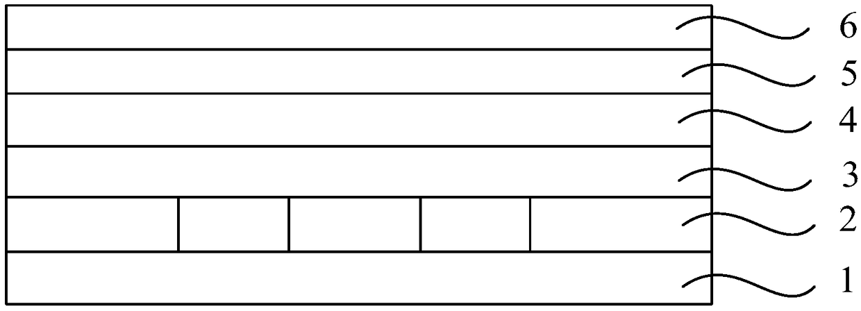
[0033] method one:
[0034] Such as figure 1 As shown, a luminescent layer 2, a cathode layer 3, a transparent conductive film layer 4, a polarizer 5 and a protective layer 6 are sequentially arranged on the base substrate 1, wherein the transparent conductive film layer 4 is directly formed on the cathode layer 3 and the cathode layer 3 Electrically connected to achieve the effect of reducing the resistance of the cathode layer 3.
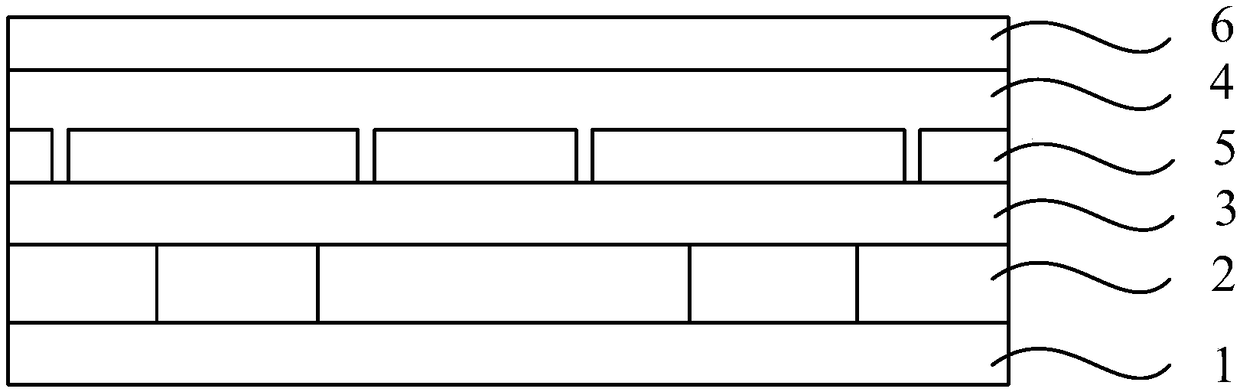
[0035] Method 2:
[0036] Such as figure 2 As shown, a light-emitting layer 2, a cathode layer 3, a polarizer 5, a transparent conductive film layer 4, and a protective film layer are sequentially arranged on the substrate 1, and a plurality of via holes are formed on the polarizer 5, and the transparent cathode layer 3 passes through the via holes. It is electrically connected to the cathode layer 3 , and the projection of the via hole on the base substrate 1 is located within the projection of the pixel definition layer on the base substrate...
PUM
 Abstract
Description
Claims
Application Information