PCB stock layout optimization method considering multiple process constraints

An optimization method and process technology, applied in the field of PCB manufacturing, can solve problems such as huge time and cost, low utilization rate, and reduced production adjustments

Inactive Publication Date: 2018-11-13
GUANGDONG UNIV OF TECH
View PDF4 Cites 9 Cited by
  • Summary
  • Abstract
  • Description
  • Claims
  • Application Information

AI Technical Summary

Problems solved by technology

Due to the particularity of PCB manufacturing, different types of PNL boards (PANEL boards, whole boards) need to make production adjustments (process adjustments, equipment adjustments, logistics adjustments, etc.) during the production process, and the time consumed by production adjustments and the cost is huge
Therefore, compared with the low utilization rate of raw materials, how to reduce production adjustment is a more difficult problem facing PCB manufacturing. To solve this problem, a method that can solve the integration and optimization of merging and layout is urgently needed Make a variety of PCBs assembled on the mother board. When all PCBs meet their respective constraints, minimize the types of final mother board assembly, reduce production adjustments, improve production efficiency, save production costs, and reduce raw material costs.

Method used


Image

  • PCB stock layout optimization method considering multiple process constraints
  • PCB stock layout optimization method considering multiple process constraints
  • PCB stock layout optimization method considering multiple process constraints

Examples


Embodiment Construction

[0051] The technical solutions of the present invention will be further described below in conjunction with the accompanying drawings and through specific implementation methods.

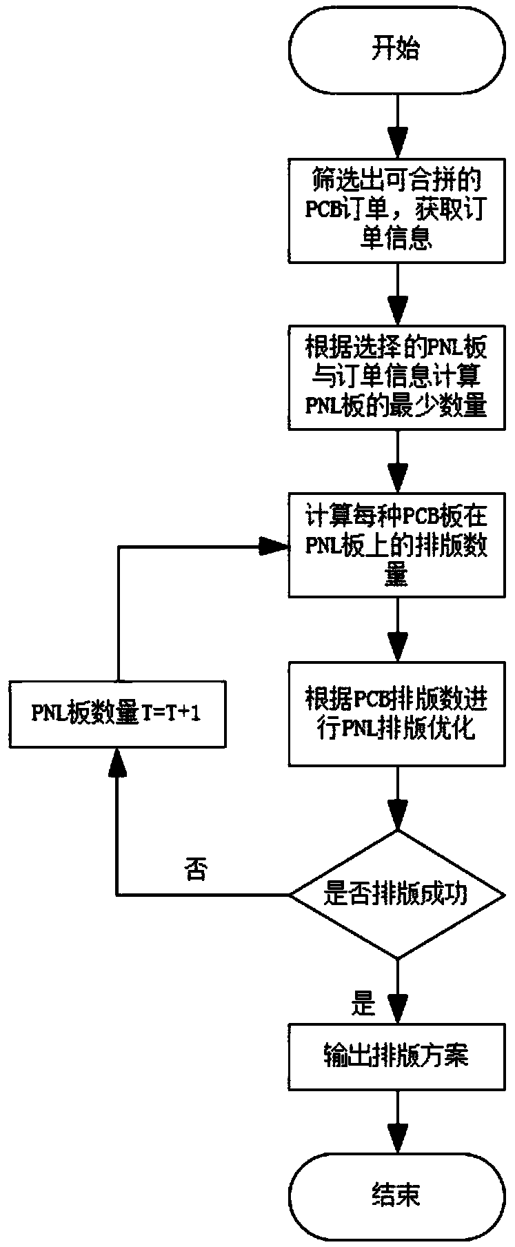
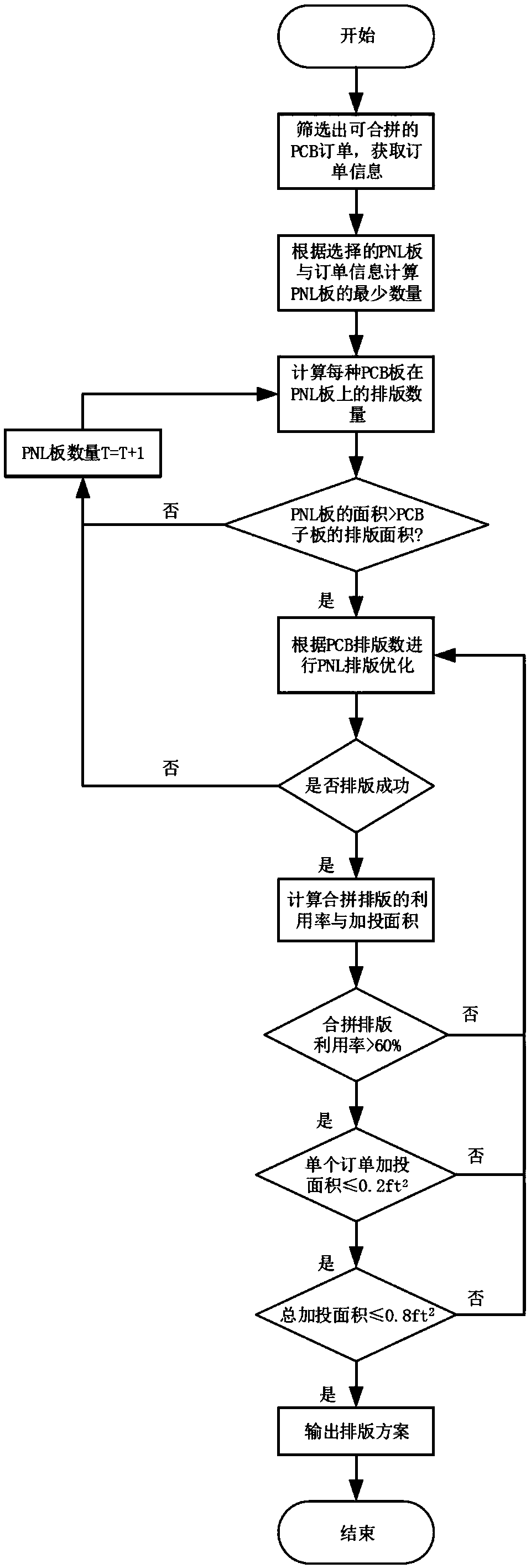
[0052] A PCB layout optimization method considering multiple process constraints in this embodiment is applied to the PCB production management system, such as figure 1 As shown, the following steps are included: Step A: Screen according to the constraint process of the PCB sub-board, and obtain the order information of n kinds of PCB sub-boards that can be assembled, and the order information includes the length l of the PCB sub-board i , width w i , delivery quantity Q i and process constraint information; step B: select a PNL plate in the PNL original film library, and then calculate the minimum required quantity T of PNL plates according to the selected PNL plate and the order information; step C: calculate each PNL plate The number of layouts required for each type of PCB sub-board P i ; Ste...


PUM


Abstract

The invention discloses a PCB stock layout optimization method considering multiple process constraints. The method comprises the following steps of step A, screening according to the constraint process of PCB daughter boards, and acquiring the order information of the PCB daughter boards which can be integrated; step B, calculating the minimum number of required PNL boards based on the PNL boardand the order information; step C, calculating the number of each type of PCB daughter boards which need layout on each PNL board; step D, carrying out single PNL layout optimization based on the layout number of each type of PCB daughter boards; step E, acquring the layout result of the step D: If the layout is successful, entering into step F; and if the layout is failed, adding 1 to the numberof the PNL boards, and then executing the step C; and step F, acquiring the best layout solution, and calculating a layout usage rate and the number of the required PNL boards. In the invention, whenthe PCB daughter boards satisfy respective constraint conditions, the number of the PNL boards is reduced, production efficiency is increased and cost is reduced.

Description

technical field [0001] The invention relates to the field of PCB manufacturing, in particular to a PCB layout optimization method considering various process constraints. Background technique [0002] In recent years, the output of PCB (Printed Circuit Board, printed circuit board) has grown more rapidly. With the rapid growth of PCB demand, PCB manufacturers have gradually changed to a large-volume, multi-variety production model. The traditional single-panel method is used to produce multiple types of PCBs. Generally speaking, each PCB is assembled into a motherboard panel, which means that more types of motherboard panels will be assembled. Due to the particularity of PCB manufacturing, different types of PNL boards (PANEL boards, whole boards) need to make production adjustments (process adjustments, equipment adjustments, logistics adjustments, etc.) during the production process, and the time consumed by production adjustments And the cost is huge. Therefore, compare...

Claims


Application Information

Patent Timeline
Patent Type & Authority Applications(China)
IPC IPC(8): H05K3/00
CPCH05K3/0097
Inventor 张浩陈新刘强冷杰武
Owner GUANGDONG UNIV OF TECH
Why Eureka
Try Eureka