Optical image capturing system
An optical imaging system, imaging surface technology, applied in optics, optical components, lenses, etc., can solve problems such as inability to meet photography requirements
- Summary
- Abstract
- Description
- Claims
- Application Information
AI Technical Summary
Problems solved by technology
Method used
Image

Examples
no. 1 example
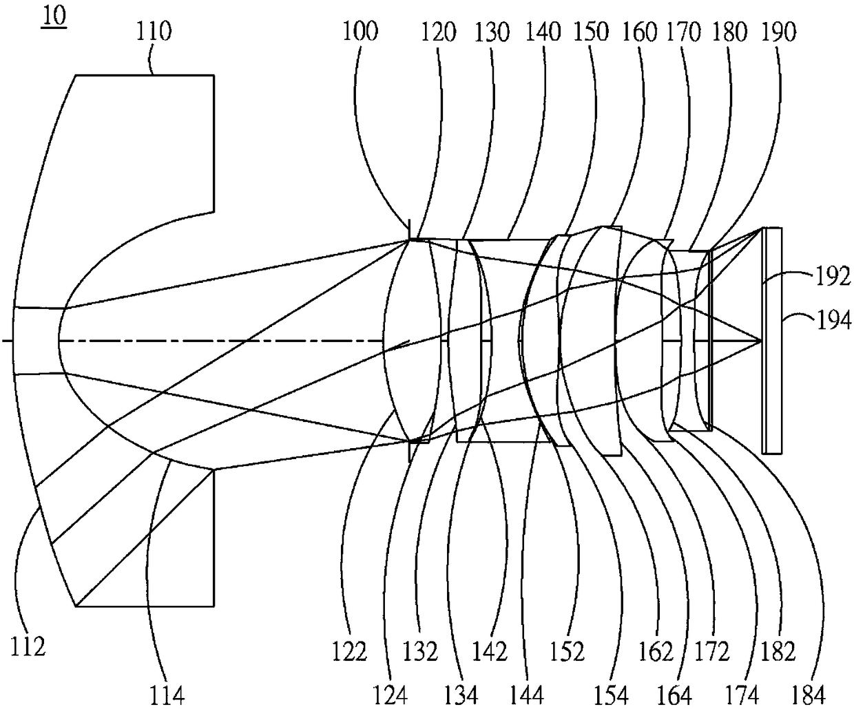
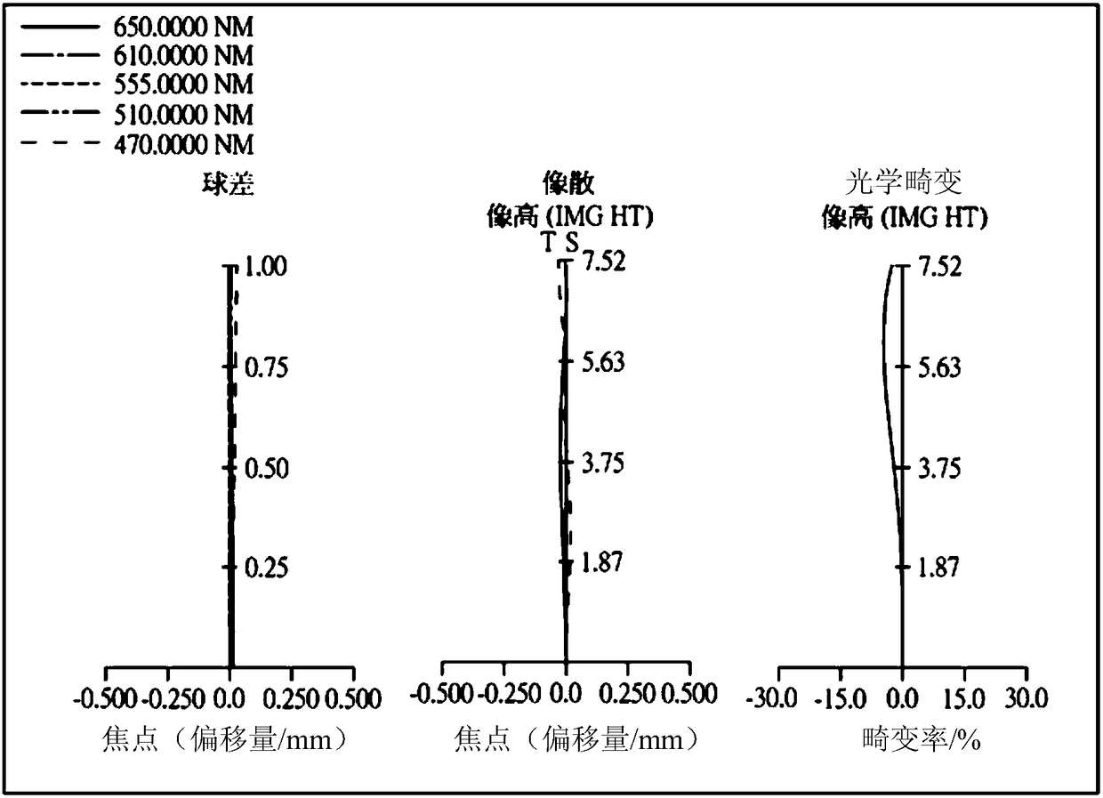
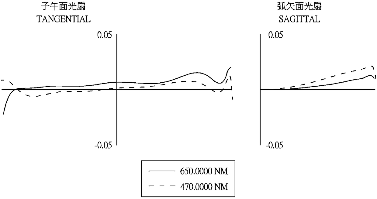
[0206] Please refer to Figure 1A and Figure 1B ,among them Figure 1A Shows a schematic diagram of an optical imaging system according to the first embodiment of the present invention, Figure 1B From left to right are the spherical aberration, astigmatism and optical distortion curves of the optical imaging system of the first embodiment. Figure 1C For the meridian surface fan and the sagittal surface fan of the optical imaging system of the first embodiment, the longest operating wavelength and the shortest operating wavelength are transverse aberration diagrams at 0.7 field of view through the edge of the aperture. Figure 1D Shows the center field of view, 0.3 field of view, and 0.7 field of view of the visible light spectrum in the embodiment of the present invention, through focus modulation conversion contrast transfer rate diagram (Through FocusMTF); Figure 1E It shows the defocus modulation conversion contrast transfer ratio diagram of the center field of view, 0.3 field...
no. 2 example
[0272] Please refer to Figure 2A and Figure 2B ,among them Figure 2A Shows a schematic diagram of an optical imaging system according to a second embodiment of the present invention, Figure 2B From left to right, the spherical aberration, astigmatism and optical distortion curves of the optical imaging system of the second embodiment are shown in sequence. Figure 2C This is a lateral aberration diagram of the optical imaging system of the second embodiment at a field of view of 0.7. Figure 2D Shows the defocus modulation conversion contrast transfer ratio diagram of the center field of view, 0.3 field of view, and 0.7 field of view of the visible light spectrum of this embodiment; Figure 2E It shows the defocus modulation conversion contrast transfer ratio diagram of the center field of view, 0.3 field of view, and 0.7 field of view of the infrared spectrum of the second embodiment of the present invention. by Figure 2A It can be seen that the optical imaging system 20 inc...
no. 3 example
[0299] Please refer to Figure 3A and Figure 3B ,among them Figure 3A Shows a schematic diagram of an optical imaging system according to a third embodiment of the present invention, Figure 3B From left to right are graphs of spherical aberration, astigmatism and optical distortion of the optical imaging system of the third embodiment. Figure 3C This is a lateral aberration diagram of the optical imaging system of the third embodiment at a field of view of 0.7. Figure 3D Shows the defocus modulation conversion contrast transfer ratio diagram of the center field of view, 0.3 field of view, and 0.7 field of view of the visible light spectrum of this embodiment; Figure 3E The defocus modulation conversion contrast transfer ratio diagram of the center field of view, 0.3 field of view, and 0.7 field of view of the infrared light spectrum of this embodiment is shown. by Figure 3A It can be seen that the optical imaging system 30 includes a first lens 310, a second lens 320, a thi...
PUM
 Abstract
Description
Claims
Application Information
 - R&D
- Intellectual Property
- Life Sciences
- Materials
- Tech Scout
- Unparalleled Data Quality
- Higher Quality Content
- 60% Fewer Hallucinations
Browse by: Latest US Patents, China's latest patents, Technical Efficacy Thesaurus, Application Domain, Technology Topic, Popular Technical Reports.
© 2025 PatSnap. All rights reserved.Legal|Privacy policy|Modern Slavery Act Transparency Statement|Sitemap|About US| Contact US: help@patsnap.com