Array substrate, repairing method thereof, display panel and display device
An array substrate and substrate substrate technology, applied in nonlinear optics, instruments, optics, etc., can solve problems such as abnormal screen display and inability to transmit signals, and achieve the effect of ensuring display effect, avoiding display abnormality, and reducing maintenance costs.
- Summary
- Abstract
- Description
- Claims
- Application Information
AI Technical Summary
Problems solved by technology
Method used
Image
Examples
Embodiment 1
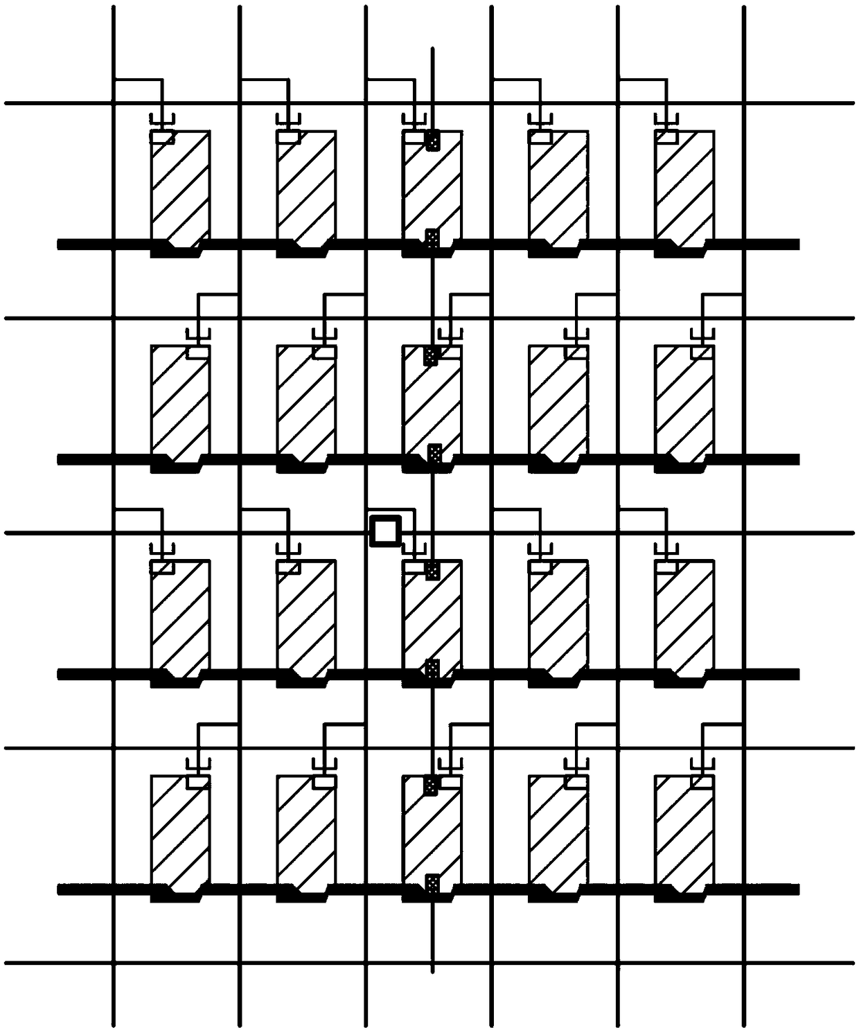
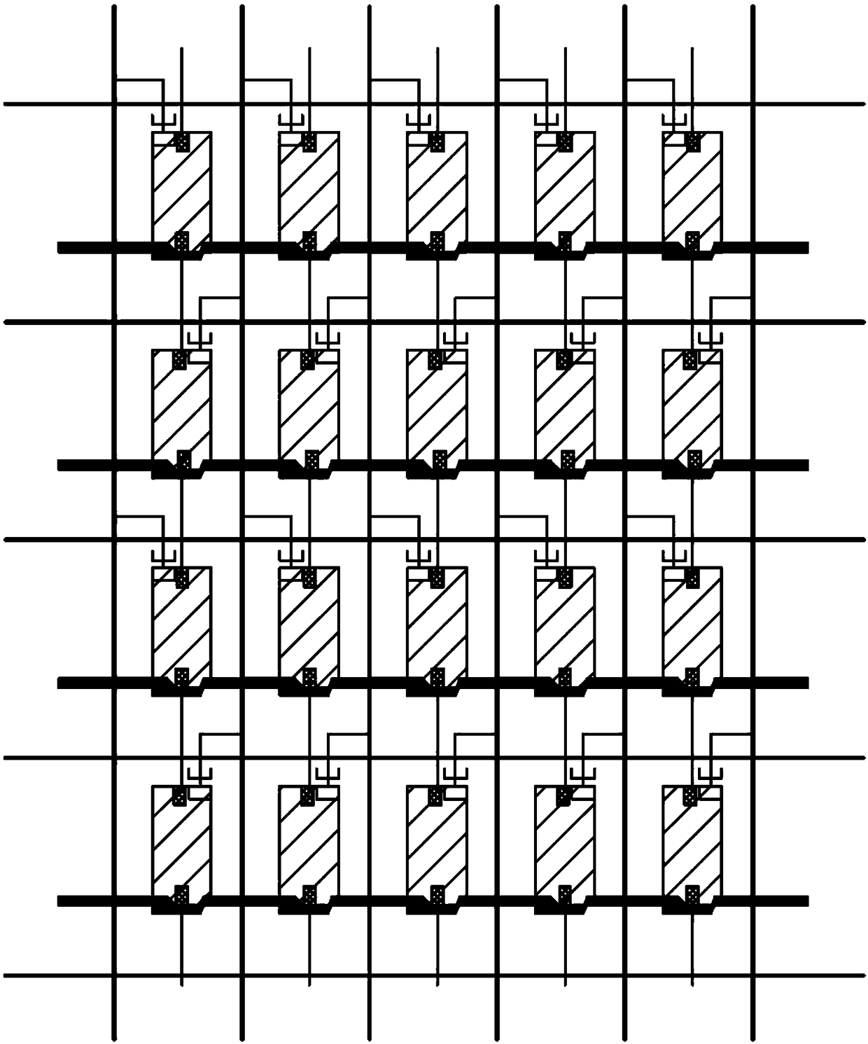
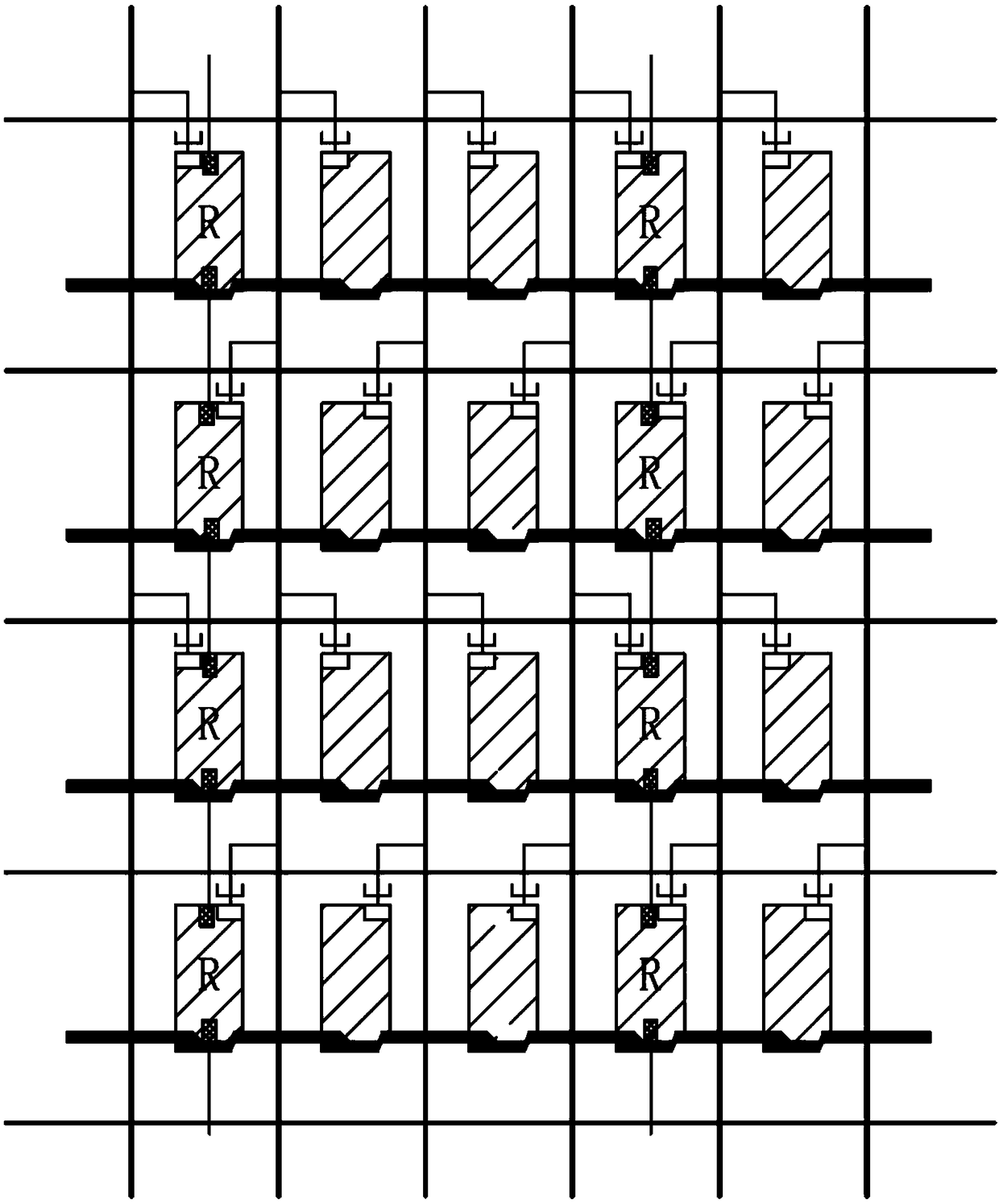
[0063] Embodiment 1: There is an open circuit between the gate line between the TFT and the data line in the pixel area i, and a common electrode line compensation structure connected to each other is provided in the pixel area of the column where the pixel area i is located, and the pixel area j is connected to the pixel Regions i are in the same column and adjacent to each other as an example for illustration. The pixel region i in this embodiment is applicable to all pixel regions in the above-mentioned 1 / 1Matrix design and the red pixel region in the 1 / 3Matrix design of the array substrate. Now step 403 includes:
[0064] The conductive path between the data line at the first end of the cutting position and the data line at the second end of the cutting position is formed by using two common electrode lines, the common electrode line compensation structure between the two common electrode lines, and the common electrode steps, including:
[0065] Connect the data line a...
Embodiment 2
[0075] Embodiment 2: There is an open circuit between the gate line between the TFT and the data line in the pixel area i, and there is no common electrode line compensation structure in the pixel area of the column where the pixel i is located, and the adjacent and adjacent to the pixel area i The pixel areas in the column where the pixel area k is located are all provided with a common electrode line compensation structure connected to each other. The pixel area t is in the same column and adjacent to the pixel area k as an example. In this embodiment, the pixel area i is suitable for an array substrate Take the green pixel area and the blue pixel area in the 1 / 3Matrix design. At this time, step 403 includes: using two common electrode lines, and the common electrode line compensation structure between the two common electrode lines and the common electrode to form the data line at the first end of the cutting position and the data line at the second end of the cutting posi...
PUM
 Abstract
Description
Claims
Application Information


