Liquid crystal display panel and display device

A technology for liquid crystal display panels and display devices, which is applied in nonlinear optics, instruments, optics, etc., and can solve problems such as light leakage in light-transmitting areas

Active Publication Date: 2018-12-11
XIAMEN TIANMA MICRO ELECTRONICS
View PDF7 Cites 20 Cited by
  • Summary
  • Abstract
  • Description
  • Claims
  • Application Information

AI Technical Summary

Problems solved by technology

[0005] Embodiments of the present invention provide a liquid crystal display panel and a display device to solve the problem of light leakage in the light-transmitting region in the prior art

Method used


Image

  • Liquid crystal display panel and display device
  • Liquid crystal display panel and display device
  • Liquid crystal display panel and display device

Examples


Embodiment 1

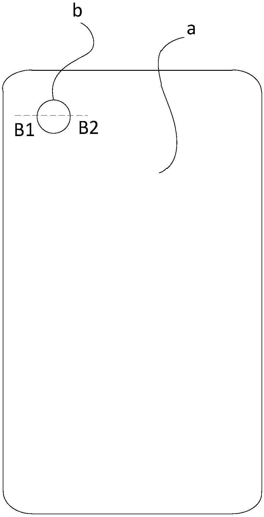
[0065] Such as Figure 4 As shown, it includes: an array substrate and an opposite substrate arranged oppositely, and a liquid crystal layer 12 located between the array substrate and the opposite substrate; the liquid crystal display panel includes a first light-transmitting area b, and a display panel surrounding the first light-transmitting area Area a; in the first light-transmitting area b, the array substrate includes a first base substrate 10, and the opposite substrate includes a second base substrate 11; the first light-transmitting area b has a first anti-reflection structure; wherein, the first The anti-reflection structure is used to reduce reflected light on the surface of the first base substrate 10 and / or the second base substrate 11 . Specifically, the first anti-reflection structure includes a first base substrate 10 and / or a second base substrate 11, that is, the first anti-reflection structure in this embodiment is the first base substrate located in the fir...

Embodiment 2

[0071] Such as Figure 5 , Figure 6 and Figure 7 As shown, it includes: an array substrate and an opposite substrate arranged oppositely, and a liquid crystal layer 12 located between the array substrate and the opposite substrate; the liquid crystal display panel includes a first light-transmitting area b, and a display panel surrounding the first light-transmitting area Area a; in the first light-transmitting area b, the array substrate includes a first base substrate 10, and the opposite substrate includes a second base substrate 11; the first light-transmitting area b has a first anti-reflection structure; wherein, the first The anti-reflection structure is used to reduce reflected light on the surface of the first base substrate 10 and / or the second base substrate 11 . Specifically, the first anti-reflection structure includes at least one first anti-reflection coating layer 13, the first anti-reflection coating layer 13 is located on the side of the first base substr...

Embodiment 3

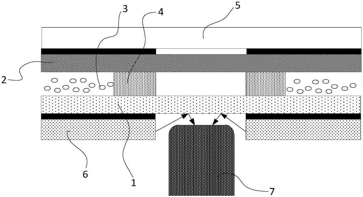
[0078] Such as Figure 8 and Figure 9As shown, it includes: an array substrate and an opposite substrate arranged oppositely, and a liquid crystal layer 12 located between the array substrate and the opposite substrate; the liquid crystal display panel includes a first light-transmitting area b, and a display panel surrounding the first light-transmitting area Area a; in the first light-transmitting area b, the array substrate includes a first base substrate 10, and the opposite substrate includes a second base substrate 11; the first light-transmitting area b has a first anti-reflection structure; wherein, the first The anti-reflection structure is used to reduce reflected light on the surface of the first base substrate 10 and / or the second base substrate 11 . Specifically, the first anti-reflection structure further includes at least a Layer the second anti-reflection coating layer 14; the thickness d3 of the second anti-reflection coating layer 14 satisfies the followin...


PUM

PropertyMeasurementUnit
thicknessaaaaaaaaaa
refractive indexaaaaaaaaaa

Abstract

The invention discloses a liquid crystal display panel and a display device. The liquid crystal display panel comprises an array substrate and an opposite direction substrate, both of which are oppositely arranged. The liquid crystal display panel also comprises a liquid crystal layer between the array substrate and the opposite direction substrate. The liquid crystal display panel comprises a first light-pervious area and a display area surrounding the first light-pervious area. In the first light-pervious area, the array substrate comprises a first substrate. The opposite direction substratecomprises a second substrate. The first light-pervious area has a first antireflection structure used for reducing reflection light of the first substrate and / or the second substrate. By arranging the first antireflection structure in the first light-pervious area, reflection light generated by light emitted from a backlight source of a display area on the first substrate and / or the second substrate is reduced. Therefore, a light leakage problem of the liquid crystal display panel in the first light-pervious area is avoided.

Description

technical field [0001] The invention relates to the field of display technology, in particular to a liquid crystal display panel and a display device. Background technique [0002] At present, display panels with a full-screen design are becoming more and more popular among consumers. The full-screen design adopts an ultra-narrow bezel design around it, combined with a panel structure designed by digging holes in the display area to place a camera. Tallest panel framing. [0003] In the liquid crystal display panel, a light-transmitting area is formed at the position of the hole, so that the camera can collect images through the light-transmitting area, but the oblique light emitted by the backlight located in the display area will propagate to the transparent substrate through structures such as transparent substrates. In the light area, the liquid crystal display panel has light leakage in the light-transmitting area, and a certain amount of light will enter the camera in...

Claims


Application Information

Patent Timeline
Patent Type & Authority Applications(China)
IPC IPC(8): G02F1/1335
CPCG02F1/133504G02F1/133507
Inventor 詹乐宇郑斌义何春燕李静邱英彰徐彬城
Owner XIAMEN TIANMA MICRO ELECTRONICS
Why Eureka
Try Eureka