Semiconductor device and manufacturing method thereof

Inactive Publication Date: 2010-07-01
SEMICON ENERGY LAB CO LTD
View PDF101 Cites 36 Cited by
  • Summary
  • Abstract
  • Description
  • Claims
  • Application Information

AI Technical Summary

Benefits of technology

[0045]A field-sequential liquid crystal display device capable o

Problems solved by technology

In the case where a liquid crystal material exhibiting a blue phase is used for a liquid crystal layer, after the display is set in white by application of voltage from black display under the state of applying no voltage, when application of voltage is stopped again, the display might not return to black completely and leakage of light might be generated; therefore, a problem of reduction in image quality and contrast might be caused.
Further, in the liquid cryst

Method used


Image

  • Semiconductor device and manufacturing method thereof
  • Semiconductor device and manufacturing method thereof
  • Semiconductor device and manufacturing method thereof

Examples


embodiment 1

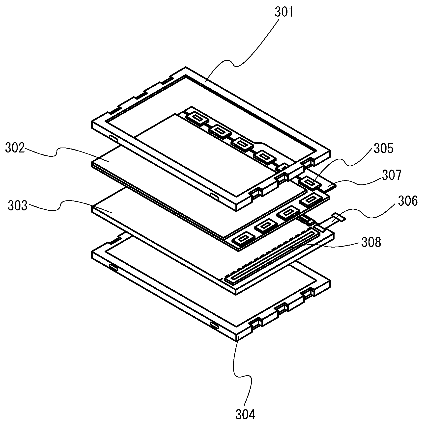
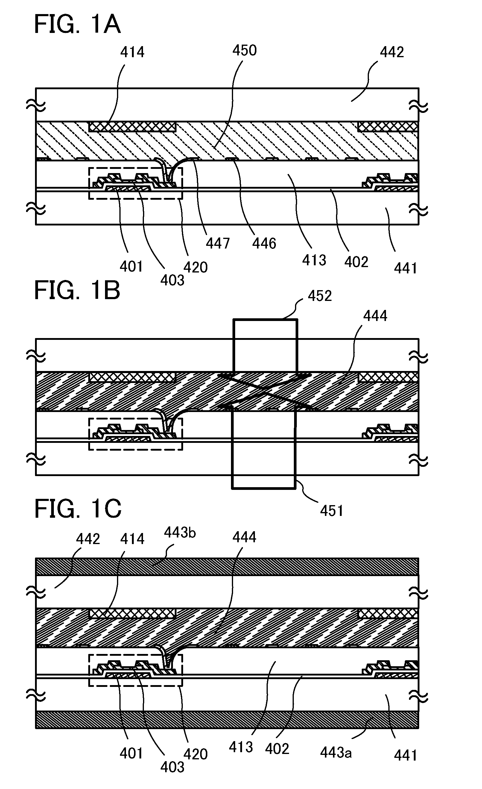
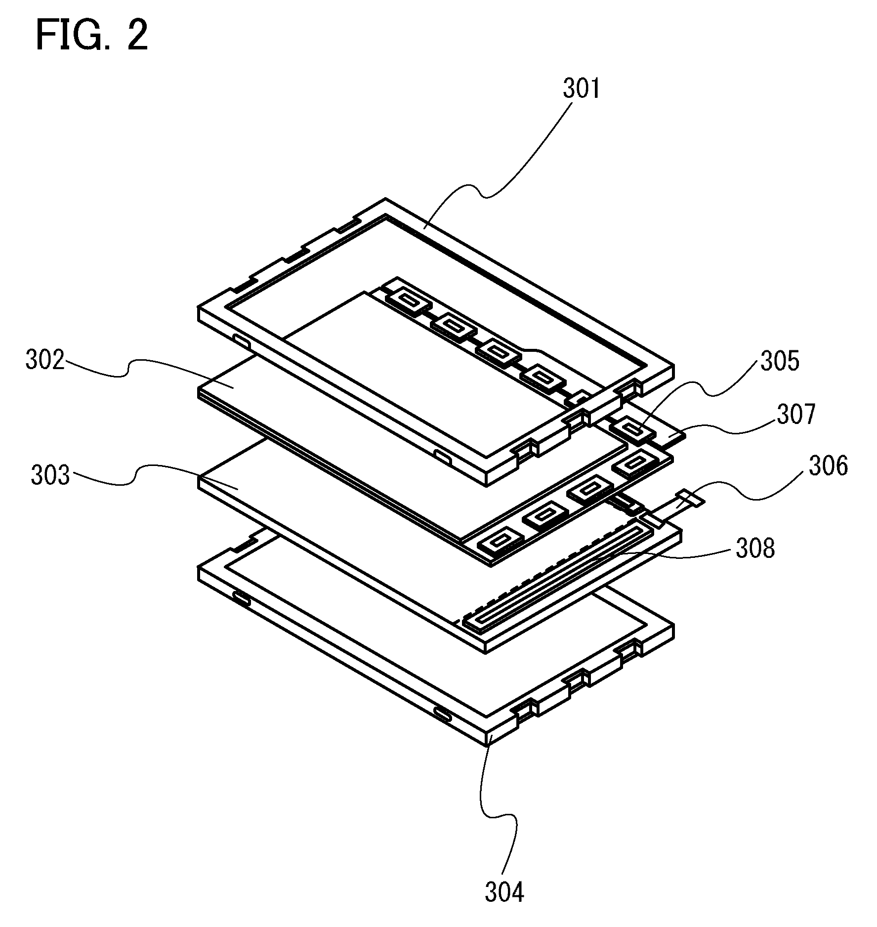
[0057]Here, a manufacturing example of a liquid crystal display device using a field-sequential system will be described below with reference to FIGS. 1A to 1C.

[0058]First, a thin film transistor (TFT) 420 that is to be a switching element is formed over a first light-transmitting substrate 441. A glass substrate is used as the first light-transmitting substrate 441. Note that a base insulating film serving as a barrier film may be provided over the first light-transmitting substrate 441. In addition, an example of using a semiconductor layer 403 for forming a channel formation region in the thin film transistor 420 will be described here.

[0059]A gate electrode layer 401 is formed over the first light-transmitting substrate 441, a gate insulating layer 402 that covers the gate electrode layer 401 is formed, and then the semiconductor layer 403 that overlaps with the gate electrode is formed over the gate insulating film 402. A material of the gate electrode layer 401 is not limited ...

embodiment 2

[0090]A liquid crystal display device will be described with reference to FIGS. 3A and 3B.

[0091]FIG. 3A is a plan view of a liquid crystal display device illustrating one pixel. FIG. 3B is a cross-sectional view taken along line X1-X2 in FIG. 3A.

[0092]In FIG. 3A, a plurality of source wiring layers (including a wiring layer 405a) are provided in parallel to each other (extended in a vertical direction in the drawing) and apart from each other. A plurality of gate wiring layers (including a gate electrode layer 401) are provided apart from each other and extend in a direction generally perpendicular to the source wiring layers (a horizontal direction in the drawing). Common wiring layers 408 are provided adjacent to the plurality of gate wiring layers and extend in a direction generally parallel to the gate wiring layers, that is, in a direction generally perpendicular to the source wiring layers (a horizontal direction in the drawing). Roughly rectangular spaces are surrounded by th...

embodiment 3

[0146]Another mode of a liquid crystal display device is illustrated in FIGS. 4A and 4B. Specifically, an example of a liquid crystal display device in which a first electrode layer with a flat shape formed below an interlayer insulating film is used as a common electrode layer and a second electrode layer having an opening pattern formed over the interlayer insulating film is used as a pixel electrode layer will be described.

[0147]FIG. 4A is a plan view of a liquid crystal display device illustrating one pixel. FIG. 4B is a cross-sectional view taken along line Y1-Y2 in FIG. 4A.

[0148]As an example, in the liquid crystal display device illustrated in FIGS. 4A and 4B, a light-blocking layer 517 is formed on the side of the first light-transmitting substrate 541, which is an element substrate, as part of an interlayer insulating film 513. A second electrode layer 546 which is electrically connected to a thin film transistor 520 serves as a pixel electrode layer, and a first electrode ...


PUM

PropertyMeasurementUnit
Photocurableaaaaaaaaaa

Abstract

It is an object to provide a liquid crystal display device capable of displaying a moving image with high image quality by employing a time-division display system (also called a field-sequential system) with the use of a plurality of light-emitting diodes (hereinafter referred to as LEDs) as a backlight. Further, it is an object to provide a liquid crystal display device in which high image quality, full color display, or low power consumption is realized by adjustment of the peak luminance. After a liquid crystal layer is sealed between a pair of substrates, polymer stabilization treatment is performed with the use of UV irradiation from both above and below the pair of substrates at the same time, whereby the polymer included in the liquid crystal layer sandwiched between the pair of substrates is evenly distributed. Thus, a liquid crystal display device is manufactured.

Description

BACKGROUND OF THE INVENTION[0001]1. Field of the Invention[0002]The present invention relates to a semiconductor device having a circuit formed using a thin film transistor (hereinafter referred to as a TFT) and a manufacturing method thereof. For example, the present invention relates to an electronic device on which an electro-optical device typified by a liquid crystal display panel is mounted as a component.[0003]In this specification, a semiconductor device refers to all types of devices which can function by utilizing semiconductor characteristics. An electro-optical device, a semiconductor circuit, and an electronic device are all included in the category of the semiconductor device.[0004]2. Description of the Related Art[0005]In recent years, a technique for forming a thin film transistor (TFT) by using a semiconductor thin film (with a thickness of approximately several nanometers to several hundreds of nanometers) formed over a substrate having an insulating surface has be...

Claims


Application Information

Patent Timeline
IPC IPC(8): G02F1/13357H01J9/20H01L33/08
CPCG02F1/133603G02F2001/13775G02F2001/13793H01L27/1225G02F1/1333G02F1/136209H01L27/1259H01L29/66969G02F1/13775G02F1/13793G02F1/137
Inventor ISHITANI, TETSUJIKUBOTA, DAISUKENISHI, TAKESHI
Owner SEMICON ENERGY LAB CO LTD
Why Eureka
Try Eureka