OLED display panel and OLED display device

A technology of display panel and display area, applied in static indicators, instruments, electrical components, etc., can solve problems such as sawtooth phenomenon, and achieve the effect of avoiding sawtooth phenomenon

Inactive Publication Date: 2018-12-11
SHENZHEN CHINA STAR OPTOELECTRONICS SEMICON DISPLAY TECH CO LTD
View PDF6 Cites 9 Cited by
  • Summary
  • Abstract
  • Description
  • Claims
  • Application Information

AI Technical Summary

Problems solved by technology

[0004] However, if the special-shaped display panel is driven by a driving circuit in the prior art, the sub-pixels in the central display area 30 and the transitional display area 40 are all driven by the same power bus, and the rectangular sub-pixels 3 in the central display area 30 It is the same as the driving voltage of the special-shaped sub-pixel 4 in the transitional display area 40, but since the area of ​​the special-shaped sub-pixel 4 in the transitional display area 40 is different from the area of ​​the sub-pixel 3 in the central display area 30, the The luminous intensity of the special-shaped sub-pixel 4 in the transitional display area 40 is different from that of the rectangular sub-pixel 3 in the central display area 30, for example: when the area of ​​the special-shaped sub-pixel 4 is smaller than the area of ​​the rectangular sub-pixel 3, in the same Driven by the driving voltage, the luminance of the special-shaped sub-pixel 4 will be smaller than the luminance of the rectangular sub-pixel. Therefore, using this kind of scheme in the prior art, the luminance difference in different regions will still produce a certain visual difference. sawtooth phenomenon

Method used


Image

  • OLED display panel and OLED display device
  • OLED display panel and OLED display device
  • OLED display panel and OLED display device

Examples


Embodiment 1

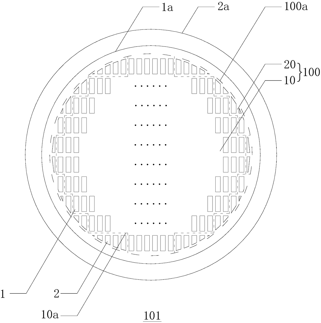
[0027] refer to figure 2 As shown (in order to avoid too many connecting lines causing too much complexity in the diagram content, figure 2 The connection lines between the following sub-pixels and the corresponding power bus are not drawn, and the other first sub-pixels 1) in the central display area 10 are omitted by ellipsis. This embodiment provides an OLED display panel 101, including special-shaped Display area 100 .

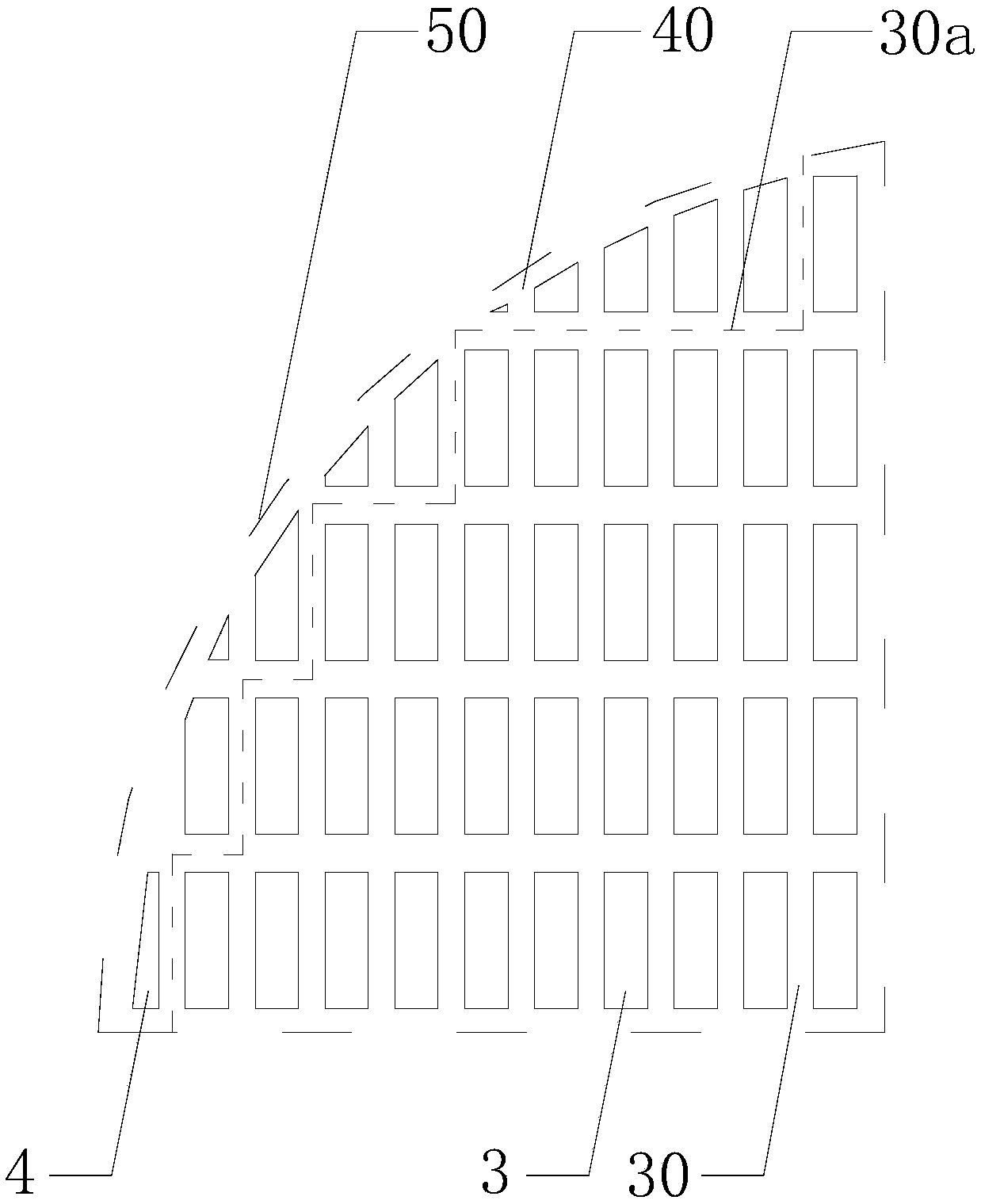
[0028] Wherein, the special-shaped display area 100 includes a central display area 10 and a transitional display area 20, the central display area 10 is provided with a plurality of first sub-pixels 1, and the edge of the central display area 10 includes a stepped area 10a, A plurality of second sub-pixels 2 are disposed in the stepped area 10 a to form the transitional display area 20 . The OLED display panel 101 is configured with a first power bus 1a and a second power bus 2a, and the first sub-pixel 1 is electrically connected to the first power b...

Embodiment 2

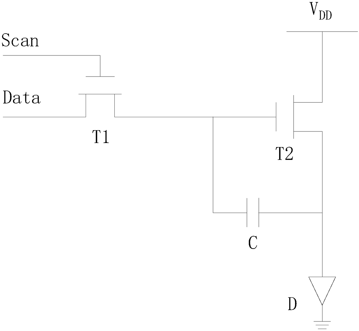
[0042] combine Image 6 As shown, the present invention also provides an OLED display device, including a driving unit 102 and an OLED display panel 101 as described in Embodiment 1, and the OLED display panel 101 includes a driving circuit layer and is connected to the driving circuit layer. The OLED display device, the driving unit 102 is connected to the driving circuit layer, the driving unit 102 inputs a driving signal to the driving circuit layer, and the driving circuit layer drives the OLED display device to display according to the driving signal An image, wherein the driving signal includes a data signal, a scanning signal and a power supply voltage signal. combine image 3 , the driving circuit of each sub-pixel is arranged in the driving circuit layer, the driving unit 102 inputs a data signal through a data line Data, the driving unit 102 inputs a scanning signal through a scanning line Scan, and the driving unit 102 inputs a scanning signal through a power bus ...


PUM


Abstract

The invention discloses an OLED display panel and an OLED display device. The OLED display panel is respectively configured with a first power bus and a second power bus, first sub-pixels of a centraldisplay area are enabled to be electrically connected to the first power bus and obtain first driving voltage from the first power bus, and second sub-pixels of a transitional display area are enabled to be electrically connected to the second power bus and obtain second driving voltage from the second power bus; and the area of the second sub-pixels is less than the area of the first sub-pixels,and the second driving voltage provided by the second power bus is higher than the first driving voltage provided by the first power bus, thereby being capable of compensating the brightness difference between the first sub-pixels and the second sub-pixels, thus enabling the brightness of the whole special-shaped display area to keep in balance, and avoiding a visual saw-tooth phenomenon caused by the brightness difference of different areas.

Description

technical field [0001] The invention relates to the technical field of organic light emitting diodes, in particular to an OLED display panel and an OLED display device. Background technique [0002] In the prior art, the display area of ​​the OLED display panel is mostly rectangular, so the sub-pixels of the OLED display panel are all designed to be rectangular. However, in the OLED special-shaped display panel, since the contour line used to define the peripheral outline of the OLED display panel often includes Arc, when it is necessary to arrange the sub-pixels along the outline of the display panel to form a special-shaped display area, such as figure 1 As shown, the rectangular sub-pixels 3 cannot completely coincide with the contour line, resulting in a stepped area 30a formed on the outer peripheral contours of adjacent rows and columns with different numbers of sub-pixels, thereby forming a visual jagged phenomenon. [0003] Generally, references such as figure 1 An...

Claims


Application Information

Patent Timeline
Patent Type & Authority Applications(China)
IPC IPC(8): G09G3/3208H01L27/32
CPCG09G3/3208H10K59/10
Inventor 周星宇
Owner SHENZHEN CHINA STAR OPTOELECTRONICS SEMICON DISPLAY TECH CO LTD
Why Eureka
Try Eureka