Display substrate and preparation method thereof, and display panel

A technology for display substrates and display areas, which is used in the manufacture of semiconductor/solid-state devices, organic semiconductor devices, electrical components, etc., can solve the problems that the yield cannot be further improved, the limited design structure, etc., to improve the design thickness and flatness, Improve the effect of encapsulation

Active Publication Date: 2018-12-18
BOE TECH GRP CO LTD
View PDF8 Cites 33 Cited by
  • Summary
  • Abstract
  • Description
  • Claims
  • Application Information

AI Technical Summary

Problems solved by technology

However, the current OLED electronic display products are limited by their own design structure, resulting in that the yield rate of packaging cannot be further improved

Method used


Image

  • Display substrate and preparation method thereof, and display panel
  • Display substrate and preparation method thereof, and display panel
  • Display substrate and preparation method thereof, and display panel

Examples


preparation example Construction

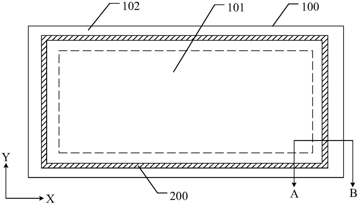
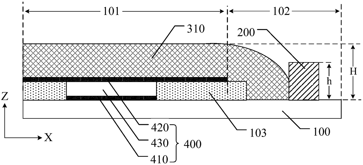
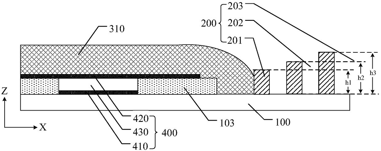
[0098] At least one embodiment of the present disclosure provides a method for preparing a display substrate, including: providing a base substrate, defining a display area of ​​the display substrate to be formed on the base substrate and a non-display area located around the display area; Forming at least one barrier dam on the base substrate in the display area; applying a first encapsulation material on the base substrate in the display area; and curing the first encapsulation material to form a first encapsulation layer, at least one of the barrier dams facing the first encapsulation layer One side thereof is liquid-repellent relative to the first encapsulating material before curing. In the display substrate obtained by the above preparation method, the barrier dam can prevent the overflow of the first encapsulation material used to obtain the first encapsulation layer, thereby improving the flatness of the first encapsulation layer, and making the display substrate can be...


PUM


Abstract

Disclosed are a display substrate and a preparation method thereof, and a display panel. The display substrate includes a display area and a non-display area located around the display area, the display substrate further comprises a substrate, and a first encapsulation layer and at least one barrier dam which are arranged on the substrate, the barrier dam is located on the substrate in the non-display region, the first encapsulation layer is located on the substrate and on one side of the at least one barrier dam facing the display region, the first encapsulation layer is formed by a cured first encapsulation material, and one side of at least one barrier dam facing the first encapsulation layer has lyophobicity compared with the first encapsulation material before curing. The barrier damscan improve the encapsulation effect of the display substrate.

Description

technical field [0001] At least one embodiment of the present disclosure relates to a display substrate, a manufacturing method thereof, and a display panel. Background technique [0002] Organic Light-Emitting Diode (OLED, Organic Light-Emitting Diode) is an organic thin film electroluminescent device, because of its simple preparation process, low cost, low power consumption, high brightness, wide viewing angle, high contrast ratio and flexible display, etc. advantages, and has attracted great attention. [0003] OLED electronic display products need to be packaged to prevent aging and damage of internal components due to the influence of infiltrated water vapor and oxygen. However, the current OLED electronic display products are limited by their own design structure, resulting in that the yield rate of packaging cannot be further improved. Contents of the invention [0004] At least one embodiment of the present disclosure provides a display substrate, including a di...

Claims


Application Information

Patent Timeline
Patent Type & Authority Applications(China)
IPC IPC(8): H01L27/32H01L51/52H01L51/56
CPCH10K59/00H10K50/84H10K71/00H10K59/124H10K59/122H10K50/844H10K2102/351H10K50/8426H10K2102/00H10K59/1201
Inventor 龙春平
Owner BOE TECH GRP CO LTD
Why Eureka
Try Eureka