LED dimming load sudden change suppression circuit
A technology of dimming circuit and load mutation, applied in the field of LED dimming load mutation suppression circuit, can solve the problems of rising working current, easy damage of LED lamp D1, rising total current of LED dimming circuit, etc. damage effect
- Summary
- Abstract
- Description
- Claims
- Application Information
AI Technical Summary
Problems solved by technology
Method used
Image
Examples
Embodiment 1
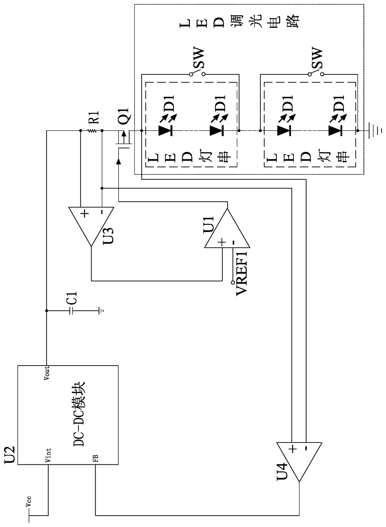
[0028] like figure 1 As shown, in Embodiment 1, the LED dimming load sudden change suppression circuit according to the present invention further includes a voltage amplifier U3 and a voltage amplifier U4, and the voltage amplifier U3 and the voltage amplifier U4 are respectively used to control the sampling resistor R1. The voltage at the terminal and the voltage between the drain and the source of the MOS transistor Q1 are collected.
[0029] Specifically, in this embodiment, the MOS transistor Q1 is a PMOS transistor; the voltage output terminal Vout of the DC-DC module U2 and one end of the capacitor C1, one end of the sampling resistor R1, and the positive phase input end of the voltage amplifier U3 The other end of the capacitor C1 is connected to the ground, the other end of the sampling resistor R1 is connected to the inverting input end of the voltage amplifier U3, the non-inverting input end of the voltage amplifier U4 and the source of the MOS transistor Q1, and th...
Embodiment 2
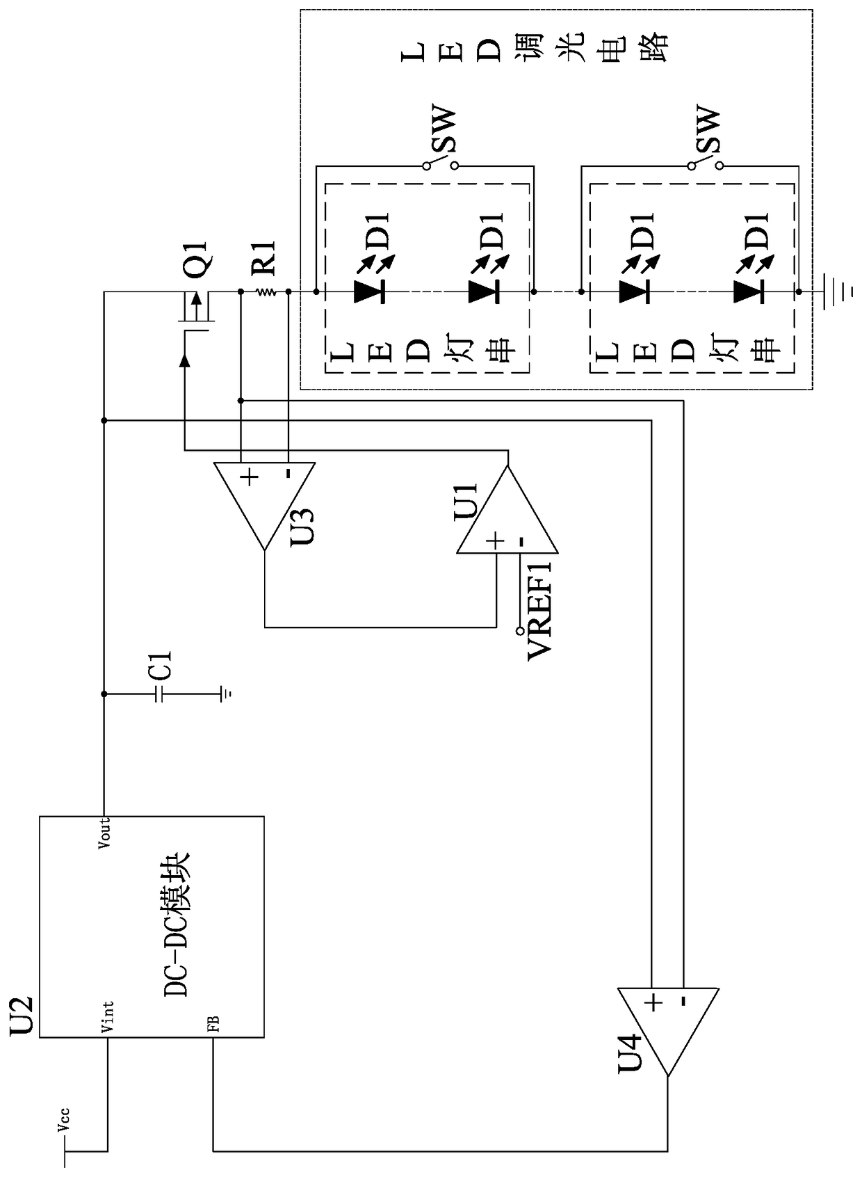
[0032] like figure 2 As shown, in the second embodiment, the LED dimming load sudden change suppression circuit according to the present invention further includes a voltage amplifier U3 and a voltage amplifier U4, and the voltage amplifier U3 and the voltage amplifier U4 are respectively used to control the sampling resistor R1. The voltage at the terminal and the voltage between the drain and the source of the MOS transistor Q1 are collected.
[0033] Specifically, in this embodiment, the MOS transistor Q1 is a PMOS transistor; the voltage output terminal Vout of the DC-DC module U2 and one end of the capacitor C1, the source of the MOS transistor Q1, and the positive phase input of the voltage amplifier U4 The other end of the capacitor C1 is connected to the ground, the drain of the MOS transistor Q1 is connected to the positive input terminal of the voltage amplifier U3, the inverting input terminal of the voltage amplifier U4 and one end of the sampling resistor R1, and...
Embodiment 3
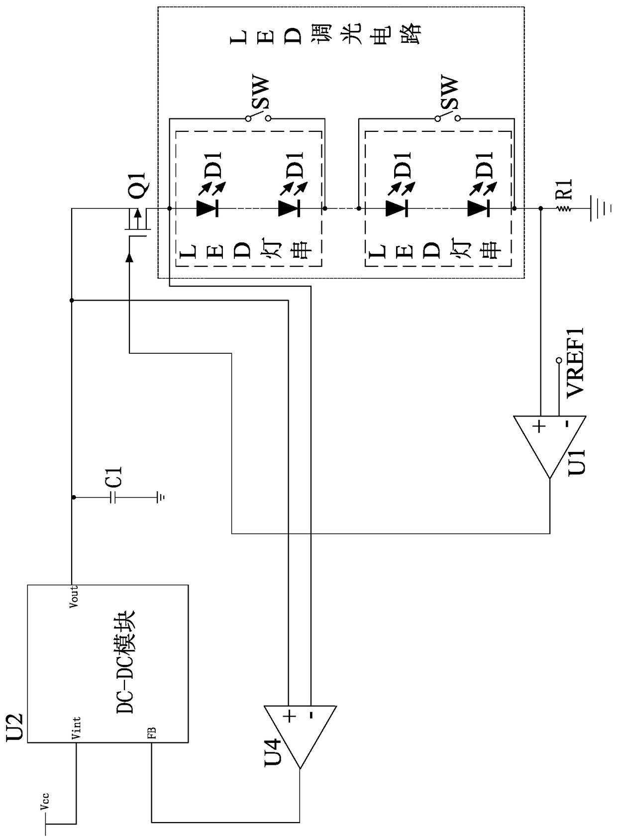
[0035] like image 3 As shown, in the third embodiment, the LED dimming load sudden change suppression circuit according to the present invention further includes a voltage amplifier U4, and the voltage amplifier U4 is used to control the voltage between the drain and the source of the MOS transistor Q1 to collect.
[0036] Specifically, in this embodiment, the MOS transistor Q1 is a PMOS transistor; the voltage output terminal Vout of the DC-DC module U2 and one end of the capacitor C1, the source of the MOS transistor Q1, and the positive phase input of the voltage amplifier U4 The other end of the capacitor C1 is connected to the ground, the drain of the MOS transistor Q1 is connected to the inverting input terminal of the voltage amplifier U4 and the input terminal of the LED dimming circuit, and the output terminal of the LED dimming circuit is connected to the sampling resistor R1 One end of the error amplifier U1 is connected to the non-inverting input end, and the oth...
PUM
 Abstract
Description
Claims
Application Information
 - R&D Engineer
- R&D Manager
- IP Professional
- Industry Leading Data Capabilities
- Powerful AI technology
- Patent DNA Extraction
Browse by: Latest US Patents, China's latest patents, Technical Efficacy Thesaurus, Application Domain, Technology Topic, Popular Technical Reports.
© 2024 PatSnap. All rights reserved.Legal|Privacy policy|Modern Slavery Act Transparency Statement|Sitemap|About US| Contact US: help@patsnap.com


