Processing method for housing assembly, housing assembly and electronic device
A shell assembly and processing method technology, applied in branch office equipment, telephone communication, electrical components, etc., can solve problems such as visual abruptness, affecting the aesthetics of electronic equipment, and failure to meet user needs, so as to reduce processing costs and improve appearance performance Power, enhance the effect of aesthetics
- Summary
- Abstract
- Description
- Claims
- Application Information
AI Technical Summary
Problems solved by technology
Method used
Image

Examples
Embodiment 1
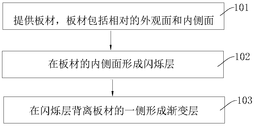
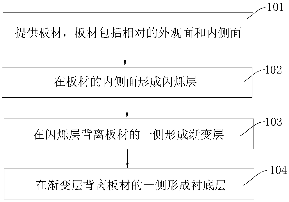
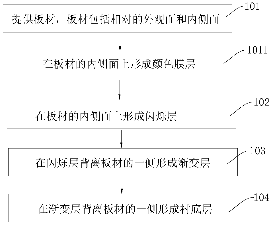
[0103] Embodiment 1: The processing method of the shell assembly 100 according to the embodiment of the present invention includes the following steps:
[0104] The inner surface 12 of the plate is hardened, and the silk screen layer 5, the color film layer 4, the scintillation layer 2, the gradient layer 3, and the substrate layer 6 are sequentially formed on the inner surface 12 of the plate, and then the plate is cut by CNC technology.
Embodiment 2
[0105] Embodiment 2: The processing method of the housing assembly 100 according to the embodiment of the present invention includes the following steps:
[0106] Harden the inner surface 12 of the plate, and sequentially form a silk screen layer 5, a color film layer 4, a scintillation layer 2, a second enhanced adhesion layer 8, a gradient layer 3, and a substrate layer 6 on the inner surface 12 of the plate, and then pass through CNC The process cuts the sheet.
Embodiment 3
[0107] Embodiment 3: The processing method of the shell assembly 100 according to the embodiment of the present invention includes the following steps:
[0108] Harden the inner surface 12 of the plate, and form the silk screen layer 5, the color film layer 4, the first enhanced adhesion layer 7, the scintillation layer 2, the gradient layer 3, and the substrate layer 6 sequentially on the inner surface 12 of the plate, and then pass through CNC The process cuts the sheet.
[0109] The casing assembly 100 according to the embodiment of the second aspect of the present invention includes: a base 1 , a scintillation layer 2 and a gradient layer 3 . The case assembly 100 may be used in an electronic device 1000 . The shell assembly 100 in this embodiment can be processed by the processing method of the shell assembly 100 according to the embodiment of the first aspect of the present invention, or can be processed by other processing methods.
[0110] Such as Figure 8 As shown...
PUM
 Abstract
Description
Claims
Application Information
PatSnap Eureka turns technology decisions into work you can execute. Powered by our Innovation Knowledge Graph, it runs expert workflows across engineering, life sciences, materials and intellectual property. Get your review-ready output in minutes.


