Stereoscopic display device
A three-dimensional display device and three-dimensional display technology, applied in optics, instruments, nonlinear optics, etc., can solve problems such as weakening moiré, affecting viewing effects, and affecting three-dimensional display effects, so as to maintain integrity and improve visual experience Effect
- Summary
- Abstract
- Description
- Claims
- Application Information
AI Technical Summary
Problems solved by technology
Method used
Image
Examples
Embodiment 2
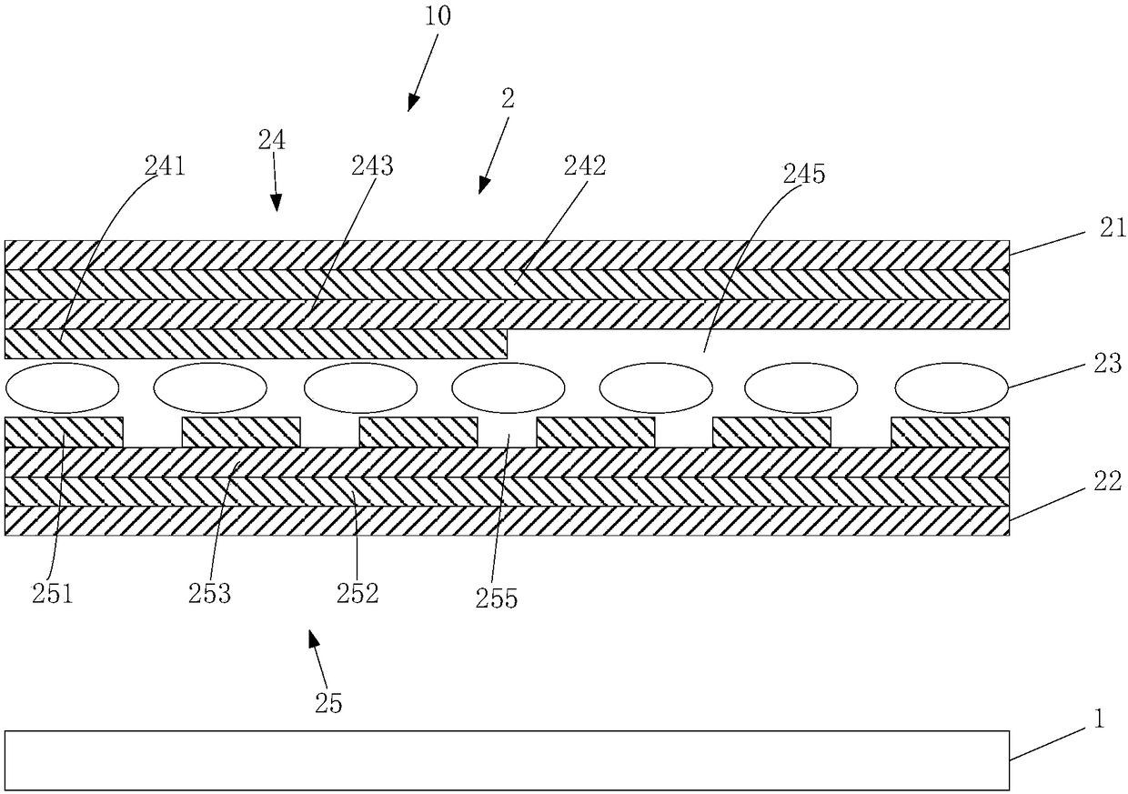
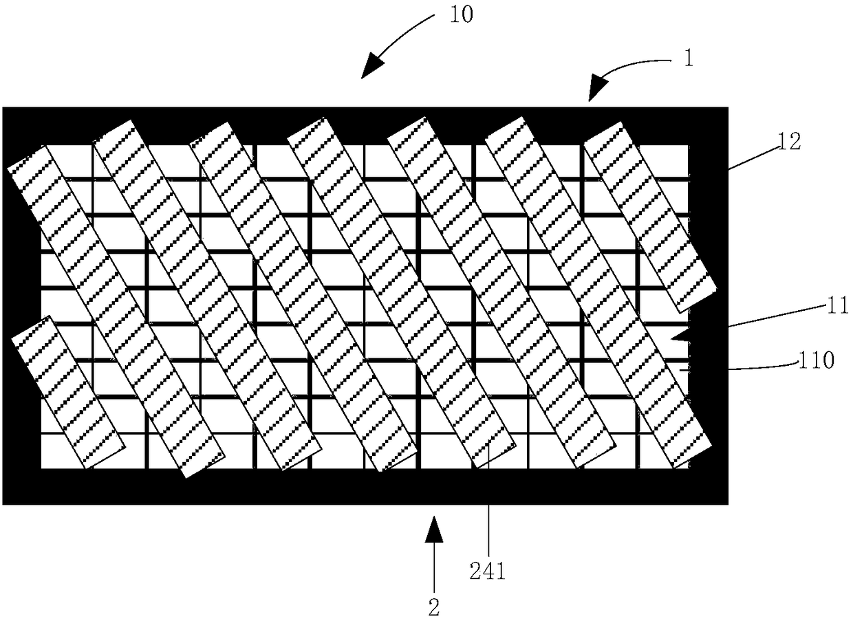
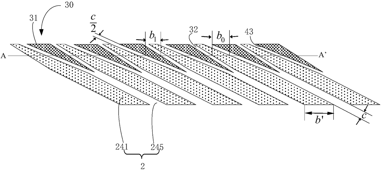
[0064] Such as Figure 6 As shown, the structure of the liquid crystal slit grating provided in this embodiment is substantially the same as the structure of the liquid crystal slit grating provided in Embodiment 1. The liquid crystal slit grating 2a includes sequentially arranged: a first substrate 21a, a liquid crystal layer 23a, and a second substrate 22a , the first substrate 21a is disposed opposite to the second substrate 22a, and the liquid crystal layer 23a is disposed between the first substrate 21a and the second substrate 22a. The first substrate 21a is provided with a first electrode layer and a second electrode layer, a first insulating layer 243a is provided between the first electrode layer and the second electrode layer, the first electrode layer includes first electrodes 241a arranged in an array, and the first electrode layer is arranged in an array. The second electrode layer is the surface electrode 242a. A third electrode layer and a fourth electrode laye...
Embodiment 3
[0068] Such as Figure 7 As shown, the structure of the liquid crystal slit grating provided in this embodiment is substantially the same as the structure of the liquid crystal slit grating provided in the second embodiment. The liquid crystal slit grating 2b includes a first substrate 21b, a liquid crystal layer 23b, a second substrate 22b, and the first substrate 21b is disposed opposite to the second substrate 22b, and the liquid crystal layer 23b is disposed between the first substrate 21b and the second substrate 22b. The side of the first substrate 21b facing the liquid crystal layer 23b is provided with a first electrode layer and a second electrode layer, a first insulating layer 243b is provided between the first electrode layer and the second electrode layer, and the first electrode layer includes an array arrangement The first electrode 241b, the second electrode layer is the surface electrode 242b. A third electrode layer and a fourth electrode layer are arranged ...
Embodiment 4
[0072] Such as Figure 8 As shown, the structure of the liquid crystal slit grating provided in this embodiment is substantially the same as the structure of the liquid crystal slit grating provided in the second embodiment. The liquid crystal slit grating 2c includes a first substrate 21c, a liquid crystal layer 23c, a second substrate 22c, and the first substrate 21c is disposed opposite to the second substrate 22c, and the liquid crystal layer 23c is disposed between the first substrate 21c and the second substrate 22c. The side of the first substrate 21c facing the liquid crystal layer 23c is provided with a first electrode layer and a second electrode layer, the second electrode layer is arranged as one layer, and a first insulating layer 243c is provided between the first electrode layer and the second electrode layer , the first electrode layer includes first electrodes 241c arranged in an array, and a first gap portion 245c is provided between two adjacent first electr...
PUM
 Abstract
Description
Claims
Application Information


