Pixel circuit and driving method thereof, array substrate

A pixel circuit and drive unit technology, applied in the field of pixel circuits, can solve problems such as the maximum brightness limit of the display panel

Active Publication Date: 2019-01-18
BOE TECH GRP CO LTD
View PDF8 Cites 2 Cited by
  • Summary
  • Abstract
  • Description
  • Claims
  • Application Information

AI Technical Summary

Problems solved by technology

[0004] The present invention at least partly solves the problem that the maximum brightness of the existing organic light emitting diode display panel is limited by the output capability of the driver chip, and provides a pixel circuit capable of obtaining higher maximum brightness while the output capability of the driver chip remains unchanged. Driving method, array substrate

Method used


Image

  • Pixel circuit and driving method thereof, array substrate
  • Pixel circuit and driving method thereof, array substrate
  • Pixel circuit and driving method thereof, array substrate

Examples


Embodiment 1

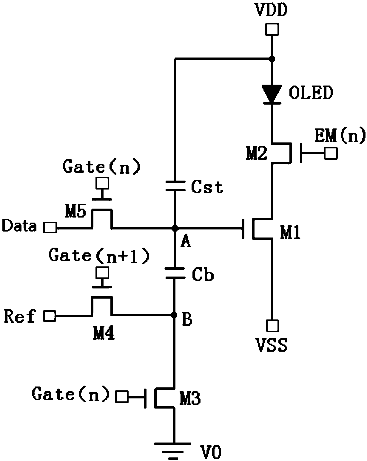
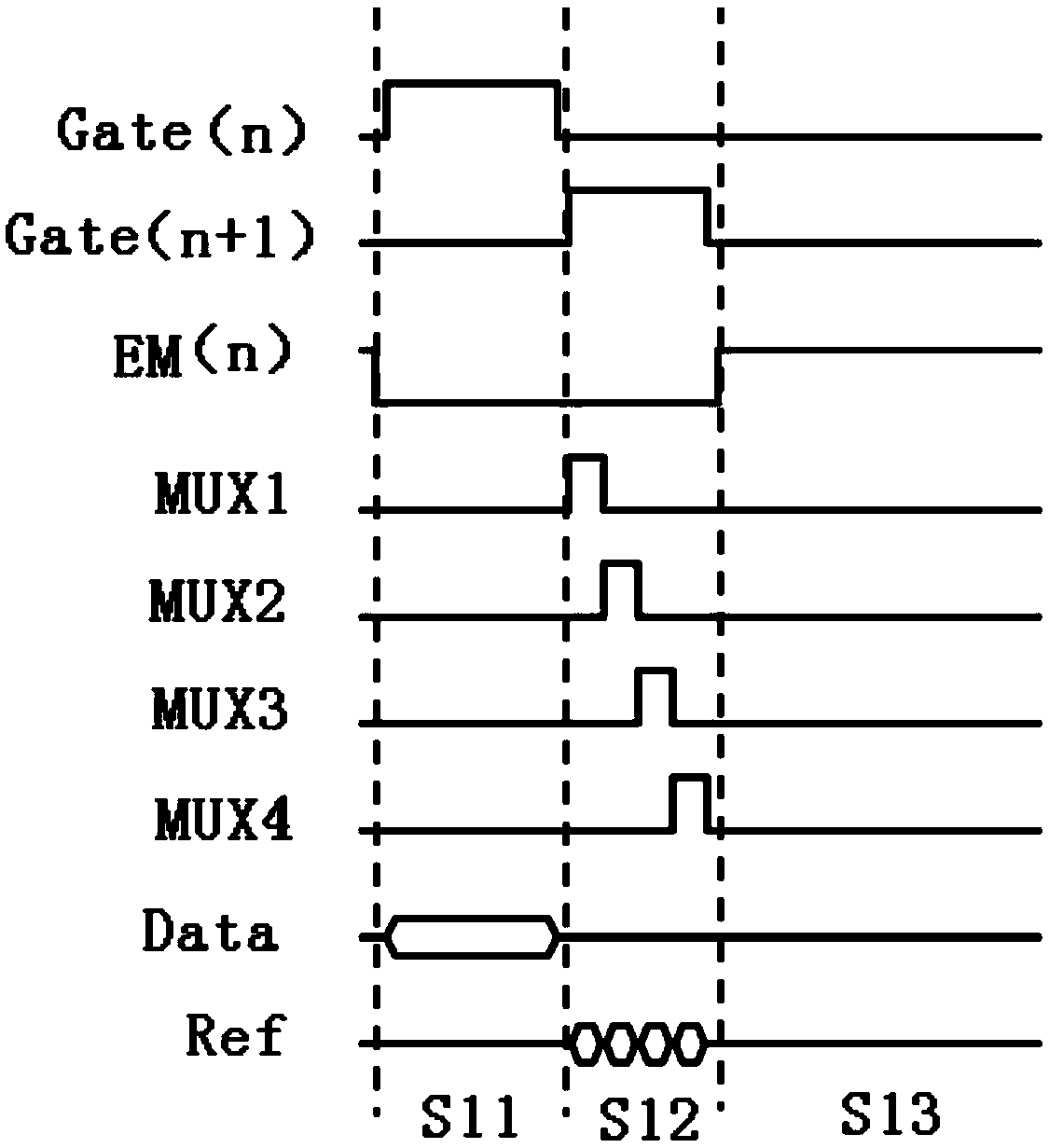
[0056] refer to Figure 1 to Figure 3 , this embodiment provides a pixel circuit.

[0057] The pixel circuit can emit light with different brightness, so it can be used in the pixels (also called sub-pixels) of the array substrate.

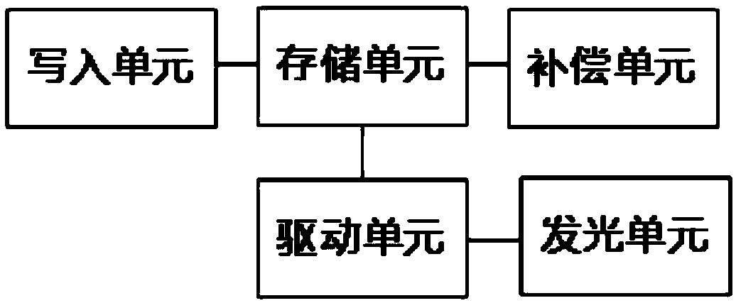
[0058] Specifically, refer to figure 1 , the pixel circuit includes:

[0059] a light emitting unit for emitting light;

[0060] The driving unit is used to drive the light emitting unit to emit light according to the driving voltage loaded on the driving unit;

[0061] a storage unit for storing the driving voltage applied to the driving unit;

[0062] a writing unit, for writing data voltage into the storage unit;

[0063] The compensation unit is used to write the compensation voltage into the storage unit, so as to obtain the driving voltage through the data voltage and the compensation voltage.

[0064]In the pixel circuit of the embodiment of the present invention, the writing unit can write the data voltage (for example, from the driv...

Embodiment 2

[0108] refer to Figure 4, this embodiment provides an array substrate, which particularly includes:

[0109] A plurality of pixel circuits 1 arranged in an array, where the pixel circuits 1 are any one of the above-mentioned pixel circuits 1 .

[0110] The array substrate includes a plurality of pixels (or sub-pixels) arranged in an array, and each pixel is provided with the above pixel circuit 1. Since the pixel circuit 1 may include an organic light emitting diode (OLED), the array substrate can be It is an organic light emitting diode array substrate.

[0111] Optionally, when the third transistor, the fourth transistor, and the fifth transistor in the pixel circuit 1 are all N-type transistors or all are P-type transistors, the array substrate further includes a plurality of data lines 4 and a plurality of gate lines 3; ,

[0112] The data voltage end of each column of pixel circuits 1 is connected to a data line 4;

[0113] The first gate voltage terminal of each row...

Embodiment 3

[0125] This embodiment provides a display panel, which includes any one of the above-mentioned display substrates.

[0126] That is to say, the above display substrate can be combined with the box substrate, driver chip, etc. to form a display panel with a display function. Wherein, when the display substrate is an OLED array substrate, the display panel is also an OLED display panel.

[0127] Specifically, the above display panel can be any product or component with a display function, such as electronic paper, mobile phone, tablet computer, television, monitor, notebook computer, digital photo frame, and navigator.


PUM


Abstract

The invention provides a pixel circuit and a driving method thereof, an array substrate, and belongs to the technical field of pixel circuits, which can at least partially solve the problem that the maximum brightness of an existing organic light emitting diode display panel is limited by the output capability of a driving chip. The pixel circuit of the embodiment of the invention comprises a light emitting unit for emitting light; A driving unit for driving the light emitting unit to emit light according to the driving voltage applied to the driving unit; A memory unit for storing a drive voltage loaded to the drive unit; A writing unit for writing a data voltage into the memory unit; A compensation unit for writing the compensation voltage to the memory unit to obtain a driving voltage by the data voltage and the compensation voltage.

Description

technical field [0001] The invention belongs to the technical field of pixel circuits, and in particular relates to a pixel circuit, a driving method thereof, and an array substrate. Background technique [0002] In HDR (High Dynamic Light Rendering) technology, the data of each image is not the gray value of each pixel (also known as sub-pixel), but its actual brightness value, so HDR technology can obtain more brightness information and achieve more Good display effect. [0003] In order to fully reflect the advantages of the HDR technology, the display panel is required to have higher maximum brightness and higher contrast (which can be achieved by increasing the maximum brightness). For an organic light emitting diode (OLED) display panel, its maximum brightness is determined by the maximum data voltage that the driver chip can provide (that is, the output capability of the driver chip), so if you want to increase its maximum brightness, you need to use a higher output...

Claims


Application Information

Patent Timeline
Patent Type & Authority Applications(China)
IPC IPC(8): G09G3/3225G09G3/3233
CPCG09G3/3225G09G3/3233
Inventor 高雪岭彭宽军
Owner BOE TECH GRP CO LTD
Why Eureka
Try Eureka