A rivet for improving the offset of a laminated layer and a method for riveting and positioning a PCB before lamination

A rivet and riveting technology, which is applied in the direction of circuit board tool positioning, circuit lamination, laminated printed circuit boards, etc., can solve the problems of increasing the fixing force after riveting, low utilization rate of plates, and low efficiency, and achieves improvement. Production efficiency, avoiding the effect of low plate utilization and avoiding waste of materials

Inactive Publication Date: 2019-01-18
SHENZHEN SUNTAK MULTILAYER PCB
View PDF4 Cites 3 Cited by
  • Summary
  • Abstract
  • Description
  • Claims
  • Application Information

AI Technical Summary

Problems solved by technology

[0006] The present invention aims at the riveting and fusion positioning methods of each layer in the pre-stacked structure in the existing PCB production and manufacturing process. For large-size backplanes such as communication substrates and thick copper power boards, slippage is likely to occur, while the PIN-lam positioning method However, there are problems such as low efficiency, low plate utilization rate, and waste of materials. A method for riveting and positioning each core layer in a pre-laminated structure can increase the fixing force after riveting, thereby improving the deviation of the laminated layers. Rivet, and the riveting positioning method before PCB pressing using the rivet

Method used


Image

  • A rivet for improving the offset of a laminated layer and a method for riveting and positioning a PCB before lamination
  • A rivet for improving the offset of a laminated layer and a method for riveting and positioning a PCB before lamination
  • A rivet for improving the offset of a laminated layer and a method for riveting and positioning a PCB before lamination

Examples


Embodiment

[0024] This embodiment provides a rivet for improving the deflection of the laminated layer, and a method for riveting and positioning a PCB using the middle rivet before crimping.

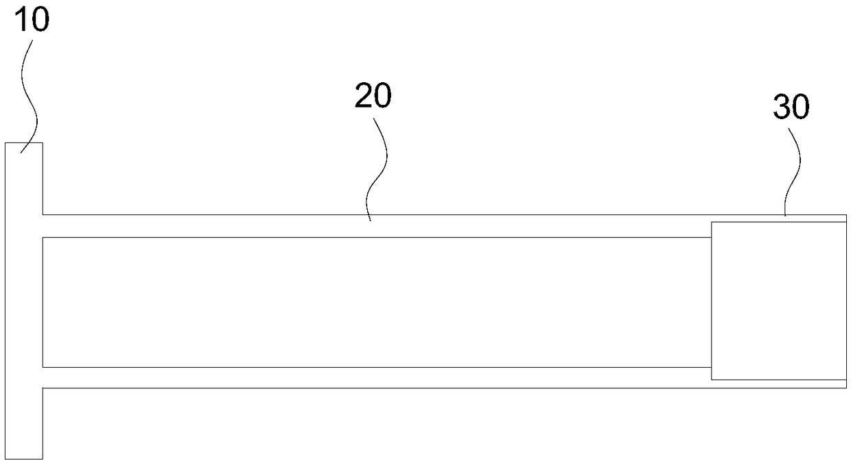
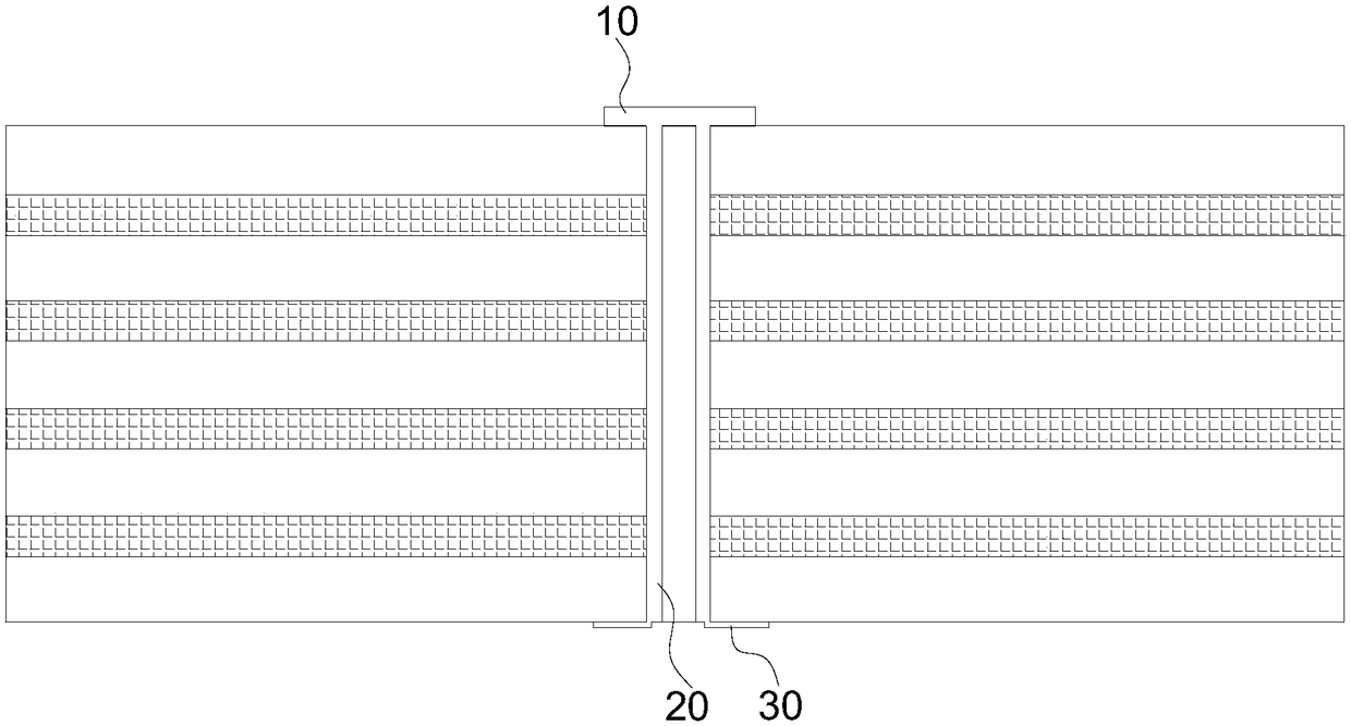
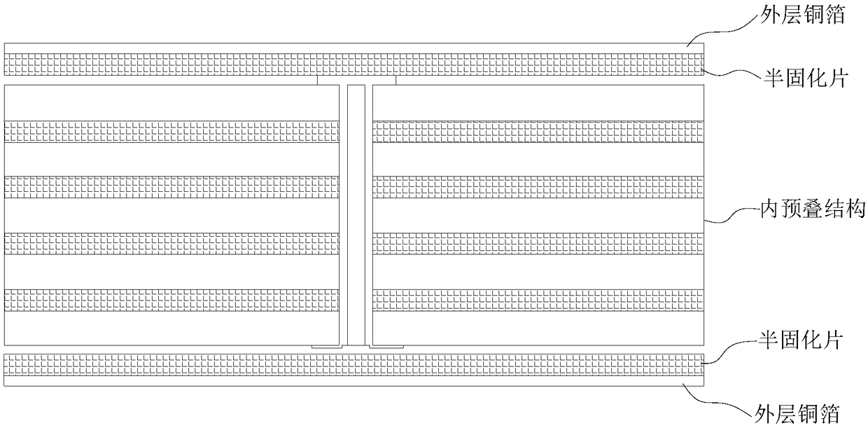
[0025] Such as figure 1 As shown, the rivet includes a nail head 10 and a nail shaft, and the nail head 10 is connected to the nail shaft. The nail bar is composed of a through section 20 and a blooming section 30 connected together, and the through section 20 and the blooming section 30 are both hollow cylinders. The wall thickness of the through section 20 of the rivet in this embodiment is 0.65mm, and the blooming section 30 is The wall thickness is 0.2mm, the length of the flowering section 30 is 1.5-2.0mm, and the length of the penetrating section 20 is 0.1mm shorter than the sum of the thickness of each core layer and the prepreg layer that need to be riveted and fixed in the pre-stacked structure, that is, the penetrating section The length of 20 is h-0.1mm, and h is the sum of the thickness o...


PUM


Abstract

The invention relates to the technical field of circuit board fabrication, in particular to a rivet for improving the offset of a laminated layer and a method for riveting and positioning a PCB beforelamination. By setting a rivet composed of a flowering section and a through section with a wall thickness not less than 0.65 mm, the rivet is used for positioning each core plate layer in the prestacking structure, the fixing force after riveting can be increased, and the deviation problem of the pressing layer can be solved. The rivet of the invention is used for riveting and fixing, and is suitable for the production and manufacture of the PCB medium-thick plate, communication substrate, thick copper power supply plate and other large-size backplates. The rivet has high alignment accuracy,can avoid the problem of internal short circuit scrap caused by deviation of the laminating layer, and can realize the compression positioning of this type of plate without using PIN-Lam positioningmethod, thereby significantly improving the production efficiency of this type of plate and avoiding the situation that PIN-Lam positioning method has the problems of low utilization rate of plate andwaste of materials.

Description

Technical field [0001] The invention relates to the technical field of circuit board manufacturing, in particular to a rivet used to improve the bias of a laminated layer and a method for riveting and positioning before a PCB is laminated. Background technique [0002] With the continuous improvement of the level and precision requirements of printed multi-layer circuit boards, a high-strength pressure (pressure generally 300-450psi) must be used to press on the pre-stacked structure of the multi-layer PCB during the pressing process. Each laminate is integrated to form a multi-layer board, and the high-strength pressure pressing on the pre-stacked structure easily causes each level in the pre-stacked structure to shift, which in turn causes the circuit properties of different networks to be connected after the shift, resulting in internal short. Therefore, each layer must be positioned before pressing. At present, there are three main positioning methods in the industry: fusion...

Claims


Application Information

Patent Timeline
Patent Type & Authority Applications(China)
IPC IPC(8): H05K3/00
CPCH05K3/0008H05K3/0058H05K2203/06
Inventor 樊锡超季辉涂圣考刘林武余秦
Owner SHENZHEN SUNTAK MULTILAYER PCB
Why Eureka
Try Eureka