Semiconductor detector and semiconductor detector manufacturing method

A technology for semiconductors and detectors, applied in the field of detectors, can solve the problems of limited influence of the electric field distribution of the detectors, single design of the pixel array unit electrodes, affecting the carrier collection capability of the detectors, etc., so as to increase the collection of carrier charges. total area, improved collection efficiency, enhanced unipolar collection characteristics

Active Publication Date: 2020-05-19
CHONGQING UNIV OF POSTS & TELECOMM
View PDF7 Cites 0 Cited by
  • Summary
  • Abstract
  • Description
  • Claims
  • Application Information

AI Technical Summary

Problems solved by technology

[0004] However, the design of the pixel array unit electrodes of the existing pixel array semiconductor radiation detectors is very single, limited to the preparation of pixel unit electrodes with different shapes and planar structures on the surface of the anode, so that the electric field distribution inside the detector is not easily affected and controlled. The specially shaped planar pixel array electrode will only cause the change of the electric field in the crystal in the area close to the pixel array electrode, which has a very limited influence on the electric field distribution in the detector, thus affecting the carrier collection ability of the detector

Method used


Image

  • Semiconductor detector and semiconductor detector manufacturing method
  • Semiconductor detector and semiconductor detector manufacturing method
  • Semiconductor detector and semiconductor detector manufacturing method

Examples


no. 1 example

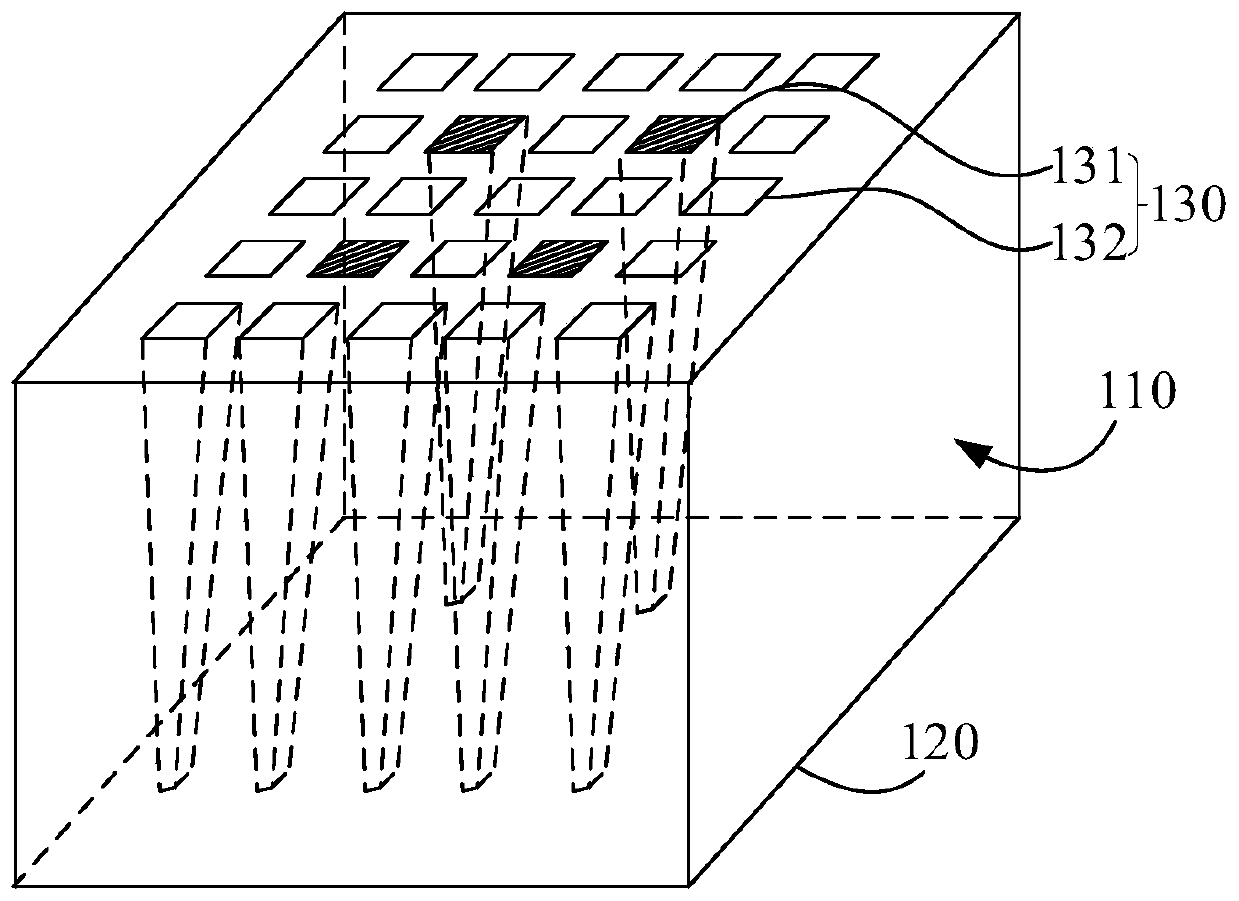
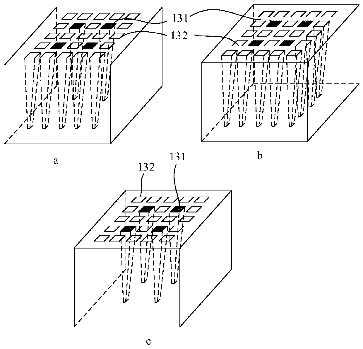
[0036] Such as figure 1 As shown, the present embodiment provides a semiconductor detector, including: a semiconductor crystal 110, a cathode 120, and an anode 130; the semiconductor crystal 110 includes a first surface and a second surface oppositely arranged on both sides of the semiconductor crystal 110; the cathode 120 Set on the first face of the semiconductor crystal 110; the anode 130 is set on the second face of the semiconductor crystal 110, the anode 130 includes: a collecting electrode 131 and a weighted gate electrode 132, and the weighted gate electrode 132 is arranged around the collecting electrode 131; wherein, the collecting electrode 131 And / or the weight grid electrode 132 is an electrode with a three-dimensional composite structure.

[0037] Specifically, the semiconductor crystal 110 serves as a detection medium of the semiconductor detector. In this embodiment, the semiconductor crystal 110 is a CdZnTe crystal. The first surface and the second surface of...

no. 2 example

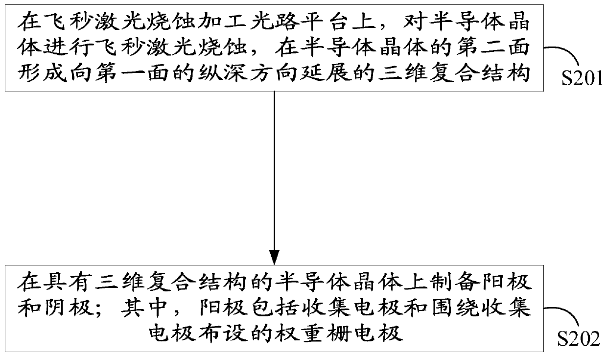
[0056] This embodiment provides a method for manufacturing a semiconductor detector, and the method is applied to prepare the semiconductor detector described in the first embodiment above.

[0057] Such as image 3 As shown, the method specifically includes the following steps:

[0058] S201. Perform femtosecond laser ablation on the semiconductor crystal on the optical path platform for femtosecond laser ablation processing, and form a three-dimensional composite structure extending in the depth direction of the first surface on the second surface of the semiconductor crystal;

[0059] S202. Prepare an anode and a cathode on a semiconductor crystal having a three-dimensional composite structure; wherein, the anode includes a collection electrode and a weighted grid electrode arranged around the collection electrode.

[0060] Specifically, before preparing the above-mentioned semiconductor detectors, it is first necessary to build such Figure 4 The optical path platform fo...


PUM


Abstract

The invention provides a semiconductor detector and a preparation method of the semiconductor detector, and relates to the technical field of detectors. The semiconductor detector comprises a semiconductor crystal, a cathode and an anode; the semiconductor crystal comprises a first face and a second face which are oppositely arranged on the two sides of the semiconductor crystal; the cathode is arranged on the first face of the semiconductor crystal; the anode is arranged on the second face of the semiconductor crystal; and the anode comprises collecting electrodes and weight gate electrodes,and the weight gate electrodes are arranged around the collecting electrodes, wherein the collecting electrodes and / or the weight gate electrodes are three-dimensional composite structure electrodes.By using the semiconductor detector, the collecting efficiency of current carriers inside the semiconductor crystal can be improved significantly.

Description

technical field [0001] The present application relates to the technical field of detectors, in particular, to a semiconductor detector and a method for preparing the semiconductor detector. Background technique [0002] Semiconductor detectors are radiation detectors that use semiconductor materials as the detection medium. The basic principle is that charged particles generate electron-hole pairs in the sensitive volume of the semiconductor detector, and the electron-hole pairs drift under the action of an external electric field to output signals. [0003] In the prior art, most semiconductor detectors adopt a detector structure with unipolar carrier collection characteristics, that is, the detector response signal is mainly the induction signal caused by electron carrier migration, which can well improve the performance of semiconductor crystal materials. Problems such as low energy resolution caused by low hole mobility. Among them, the pixel array semiconductor radiat...

Claims


Application Information

Patent Timeline
Patent Type & Authority Patents(China)
IPC IPC(8): G01T1/36G01T1/24
CPCG01T1/241G01T1/244G01T1/366
Inventor 黎淼刘涵曾弘宇姚童谢应涛何丰
Owner CHONGQING UNIV OF POSTS & TELECOMM
Why Eureka
Try Eureka