Test structure and manufacturing method thereof

A technology for testing structures and manufacturing methods, applied in the field of semiconductors, to achieve the effect of improving WAT test failures

Active Publication Date: 2019-03-05
SEMICON MFG INT (SHANGHAI) CORP +1
View PDF10 Cites 4 Cited by
  • Summary
  • Abstract
  • Description
  • Claims
  • Application Information

AI Technical Summary

Problems solved by technology

[0004] However, the inventors of the present application have found that when the WAT test is carried out to the bonded test structure, the WAT test failure is more frequent

Method used


Image

  • Test structure and manufacturing method thereof
  • Test structure and manufacturing method thereof
  • Test structure and manufacturing method thereof

Examples


Embodiment Construction

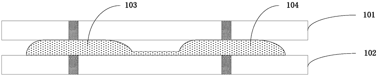
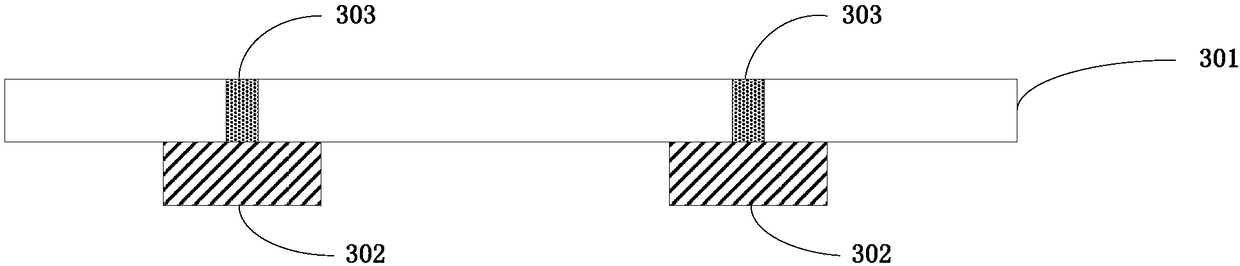
[0039] Various exemplary embodiments of the present application will now be described in detail with reference to the accompanying drawings. It should be understood that, unless specifically stated otherwise, the relative arrangement of components and steps, numerical expressions and numerical values ​​set forth in these embodiments should not be construed as limiting the scope of the present application.

[0040] In addition, it should be understood that, for ease of description, the dimensions of the various components shown in the drawings are not necessarily drawn in accordance with actual proportional relationships. For example, the thickness or width of some layers may be exaggerated relative to other layers.

[0041] The following description of the exemplary embodiments is merely illustrative, and in no sense is not regarded as any restriction on the application and its application or use.

[0042] The technologies, methods, and devices known to those of ordinary skill in the...


PUM


Abstract

The application discloses a test structure and a manufacturing method thereof, and relates to the technical field of semiconductors. The method comprises the following steps: providing a top wafer structure, wherein the top wafer structure comprises a top wafer and a plurality of first bonding pads which are arranged at the bottom of the top wafer at intervals; providing a bottom wafer structure,wherein the bottom wafer structure comprises a bottom wafer and a plurality of second bonding pads which are arranged on the top of the bottom wafer at intervals, and the side face of at least one second bonding pad in adjacent two second bonding pads is provided with an insulating layer; and bonding the plurality of first bonding pads and the plurality of second bonding pads in a eutectic bondingway, wherein each first bonding pad is bonded with each second bonding pad to form a plurality of bonding pads. Through adoption of the manufacturing method, the problem concerned with connection ofbonded bonding pads can be solved.

Description

Technical field [0001] This application relates to the field of semiconductor technology, in particular to a test structure and a manufacturing method thereof. Background technique [0002] The wafer acceptance test (WAT test) is an electrical test for various test structures on the wafer after all the manufacturing processes are completed on the wafer. [0003] MEMS sensors such as microelectromechanical systems (MEMS) inertial sensors have a process of eutectic bonding of two wafers. There are test structures in the dicing lanes of the top wafer and the bottom wafer. The top wafer and the bottom wafer are eutectic bonded to form a bonded test structure, and then the bonded test structure can be WAT tested. [0004] However, the inventor of the present application found that when the WAT test is performed on the bonded test structure, the WAT test fails more frequently. Summary of the invention [0005] An object of the present application is to provide a test structure and a manuf...

Claims


Application Information

Patent Timeline
Patent Type & Authority Applications(China)
IPC IPC(8): B81B7/00B81B7/02B81C3/00B81C99/00
CPCB81B7/0012B81B7/02B81C3/001B81C99/0045B81B2201/02G01R31/2812G01R31/2829G01R31/2831G01R31/2844H01L22/34B81C1/00333B81B7/0077B81C1/00269H01L24/64H01L24/89B81B2201/0292G01R31/26
Inventor 毛益平李广宁
Owner SEMICON MFG INT (SHANGHAI) CORP
Why Eureka
Try Eureka