Universally-applicable wafer measurement fixture with metal frame

A wafer and jig technology, which is applied in the field of shared measurement jig for iron frame wafers, can solve the problems of manual placement of dimensional errors, large deviations, affecting test operations, etc., to improve accuracy, work efficiency and quality. Effect

Inactive Publication Date: 2019-03-08
合肥新汇成微电子股份有限公司
View PDF1 Cites 0 Cited by
  • Summary
  • Abstract
  • Description
  • Claims
  • Application Information

AI Technical Summary

Problems solved by technology

[0002] The basic process of traditional packaging is wafer thinning, ball planting, chip scribing, finished product testing, and chip picking and packaging. Due to the high requirements for chip placement during finished product testing, the err

Method used


Image

  • Universally-applicable wafer measurement fixture with metal frame
  • Universally-applicable wafer measurement fixture with metal frame
  • Universally-applicable wafer measurement fixture with metal frame

Examples


Embodiment Construction

[0013] The technical solutions in the embodiments of the present invention will be clearly and completely described below in conjunction with the embodiments of the present invention. Apparently, the described embodiments are only some of the embodiments of the present invention, not all of them. Based on the embodiments of the present invention, all other embodiments obtained by persons of ordinary skill in the art without making creative efforts belong to the protection scope of the present invention.

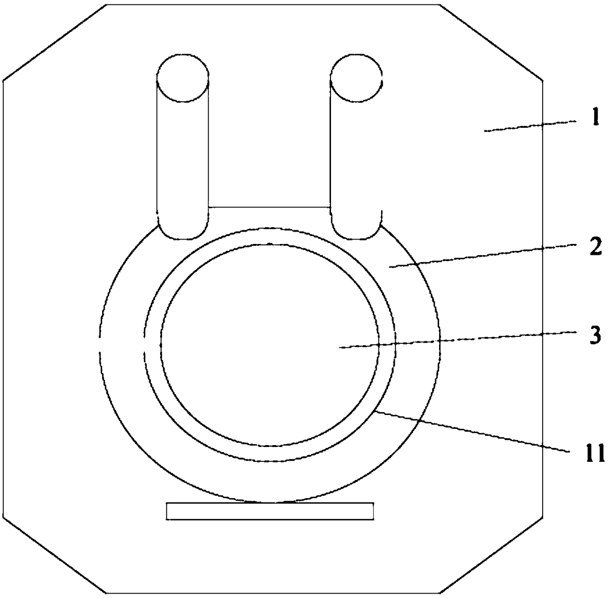
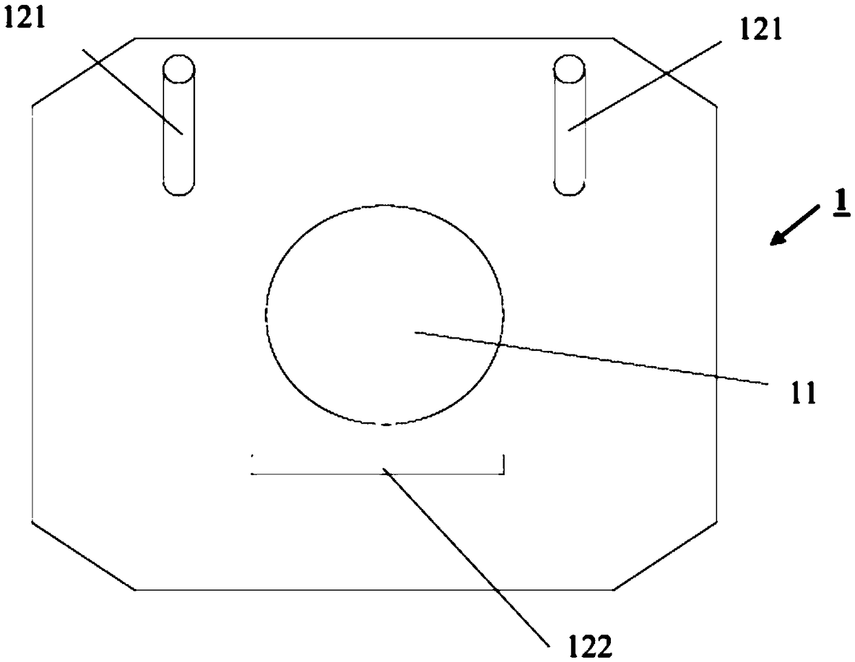
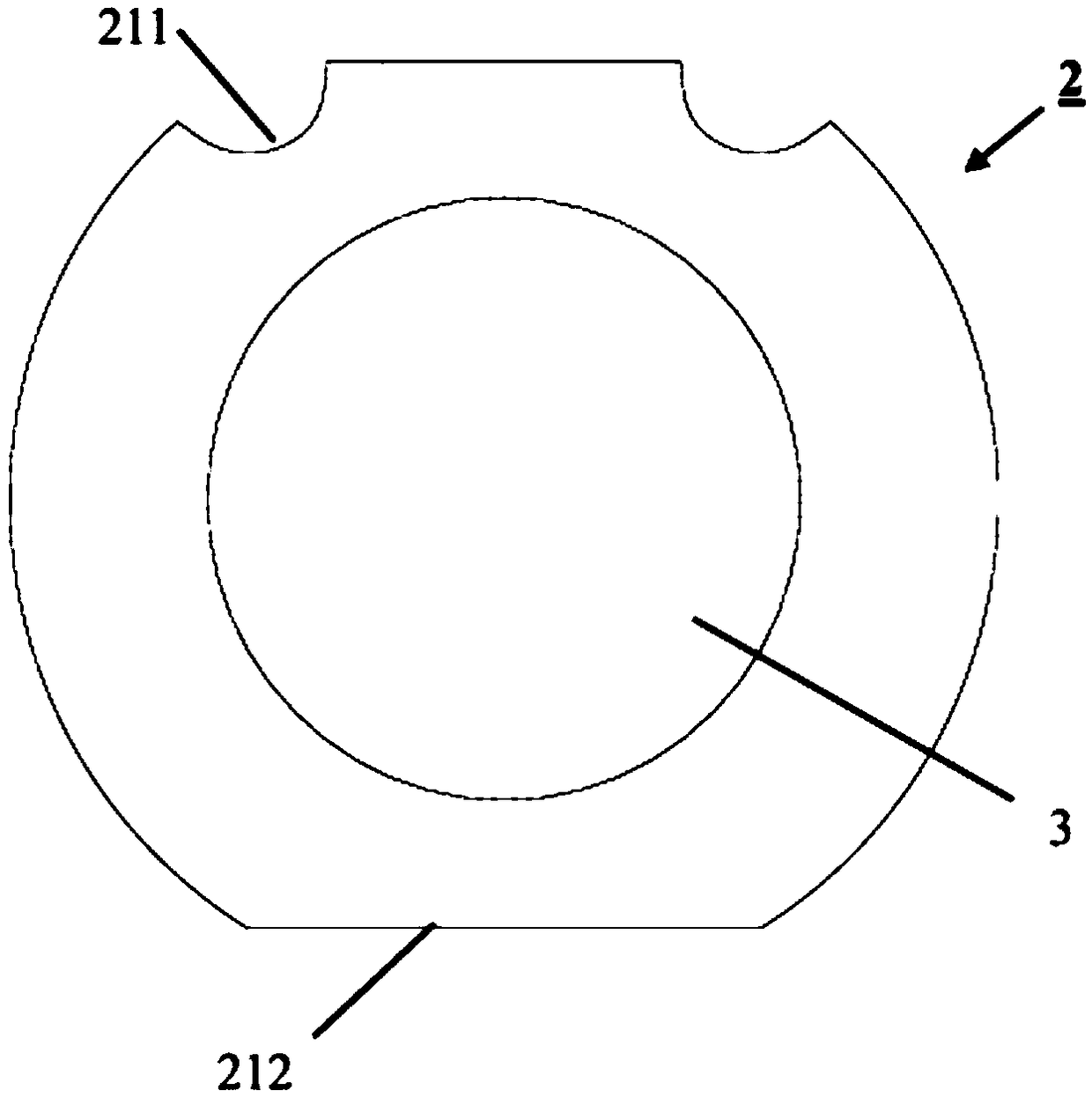
[0014] The invention relates to a common measurement fixture for wafers with iron frames, see Figure 1 to Figure 3 , including a carrying platform 1 and a wafer support 2, a circular reference line 11 is formed on the surface of the carrying platform 1, and a plurality of positioning protrusions fixedly arranged around the reference line 11, the wafer support 2 It is a transparent plate-like structure with a mounting area for mounting wafers. The outer periphery of the wafer...


PUM


Abstract

The invention discloses a universally-applicable wafer measurement fixture with a metal frame. The measurement fixture comprises a carrying platform and a wafer holder; a circular reference line is formed on the surface of the carrying platform; a plurality of positioning protrusions are fixedly arranged around the circular reference line; the wafer holder is of a transparent plate-like structureand is provided with a mounting area for mounting a wafer; the outer circumference of the wafer holder is provided with positioning surfaces matched with the positioning protrusions; and the positioning protrusions include columnar protrusions and a rectangular protrusion, and the positioning surfaces include curved surfaces and a planar surface correspondingly.

Description

technical field [0001] The invention belongs to the technical field of semiconductors, and in particular relates to a common measuring fixture for wafers with an iron frame. Background technique [0002] The basic process of traditional packaging is wafer thinning, ball planting, chip scribing, finished product testing, and chip picking and packaging. Due to the high requirements for chip placement during finished product testing, the error range is generally within a few millimeters. Due to the size error of the wafer ring itself and the error caused by manual wafer placement, the deviation is often too large, which affects the test operation. Contents of the invention [0003] The object of the present invention is to provide a common measurement jig for wafers with an iron frame. [0004] The present invention is achieved through the following technical solutions: [0005] A common measurement fixture for wafers with an iron frame, including a carrying platform and a ...

Claims


Application Information

Patent Timeline
IPC IPC(8): G01B5/00
CPCG01B5/00G01B5/0002
Inventor 许刚钟志芳
Owner 合肥新汇成微电子股份有限公司
Why Eureka
Try Eureka