

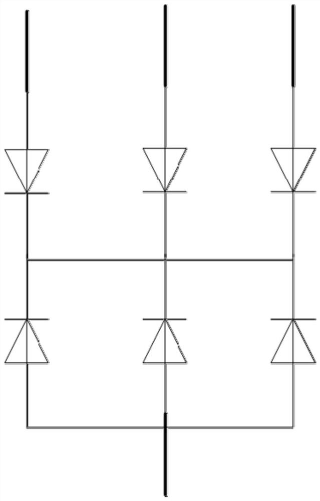
A power device protection chip and its manufacturing method
A technology of a power device and a manufacturing method, applied in the field of power device protection chips, can solve the problems of complex chip design and unfavorable packaging, and achieve the effects of reducing packaging and manufacturing costs, facilitating and rapid packaging, and reducing parasitic capacitance.
- Summary
- Abstract
- Description
- Claims
- Application Information
AI Technical Summary
Problems solved by technology
Method used
Image


Examples
Embodiment Construction
[0018] The principles and features of the present invention are described below in conjunction with the accompanying drawings, and the examples given are only used to explain the present invention, and are not intended to limit the scope of the present invention.
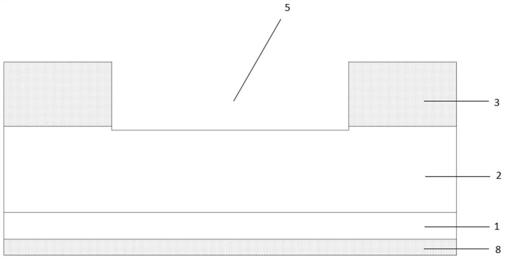
[0019] Such as Figure 5 Shown, the technical means that the present invention adopts is as follows:
[0020] A power device protection chip, the power device protection chip includes a substrate 1 of a first conductivity type, a first epitaxial layer 2 of a first conductivity type, an injection region 4 of a second conductivity type, a second epitaxial layer 3, and a trench Groove 5, silicon oxide layer 6 and first metal layer 7, the first epitaxial layer 2 is formed on the upper surface of the substrate 1, the implantation region 4 is formed downward from the upper surface of the first epitaxial layer 2, and the second epitaxial layer 3 is formed On the upper surface of the first epitaxial layer 2, a trench 5 ext...
PUM
 Abstract
Description
Claims
Application Information