
Mask plate, display substrate and manufacturing method thereof, display panel

A technology for display substrates and masks, which is applied in the photolithographic process of patterned surfaces, semiconductor/solid-state device manufacturing, instruments, etc., and can solve the problem of strict masking process requirements at the edge of display substrates and a large number of film masks , high process cost and other issues

Active Publication Date: 2021-10-08
BOE TECH GRP CO LTD +1
View PDF5 Cites 0 Cited by
  • Summary
  • Abstract
  • Description
  • Claims
  • Application Information

AI Technical Summary

Problems solved by technology

However, when changing the size of the backplane thin-film transistor, the number of film masks needs to be changed is large, and the mask process requirements for the edge of the display substrate are strict, the operation is complicated, and the process cost is high.

Method used


Image

  • Mask plate, display substrate and manufacturing method thereof, display panel
  • Mask plate, display substrate and manufacturing method thereof, display panel
  • Mask plate, display substrate and manufacturing method thereof, display panel

Examples


Embodiment Construction

[0044] Specific embodiments of the present invention will be described in detail below in conjunction with the accompanying drawings. It should be understood that the specific embodiments described here are only used to illustrate and explain the present invention, and are not intended to limit the present invention.

[0045] After repeated studies, the inventors of the present invention found that the reasons for the step effect at the edge of the display area of ​​the existing display panel are as follows:

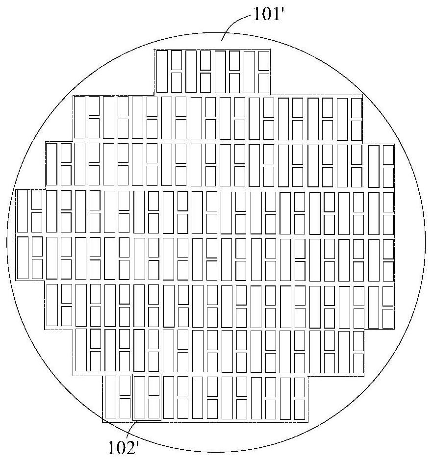
[0046] In the display panel in the prior art, the edges of the pixel units are mostly straight lines, such as figure 1 As shown, the edges of the pixel units 102' in each row are straight sides, and for a display panel with curved edges, there must be gaps between the pixel units whose edges are straight lines and the curved edges of the display panel without pixel units. The blank area 101 ′, which results in that when the display panel is displaying, the blank area 10...


PUM

PropertyMeasurementUnit
widthaaaaaaaaaa

Abstract

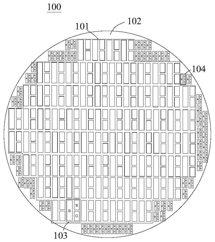
The present invention provides a display substrate, at least a part of the edge of the display substrate is arc-shaped, the display substrate includes a main display area, a plurality of rows of main pixel units are arranged in the main display area, and each row of main pixel units includes a plurality of main pixel units At least one edge pixel unit is disposed in the space between the row edge of the main pixel unit corresponding to the arc-shaped edge of the display substrate and the arc-shaped edge, and the shape of the main pixel unit is different from that of the edge pixel unit. The present invention also provides a mask plate for making a display substrate, a method for making a display substrate by using the mask plate, and a display panel including the display substrate. Edge pixel units are arranged on the edge of the display substrate, which can increase the lighting area of ​​the edge of the display area, thereby improving the step effect of the edge of the display area of ​​the display panel and enhancing the display effect.

Description

technical field [0001] The present invention relates to the field of display technology, in particular, to a display substrate, a mask for manufacturing the display substrate, a method for manufacturing the display substrate by using the mask, and a display panel including the display substrate . Background technique [0002] When the existing display panel with a circular or rounded display area is displayed, the display brightness is low at the edge of the display area of ​​the display panel, and the display brightness is high at the middle part of the display area, and obvious steps or jagged edges appear at the edge of the display area. Shaped burrs, known as the ladder effect in the industry, seriously affect the display effect. [0003] In the prior art, brightness correction is performed by changing the size of the backplane thin film transistor (TFT) to change its parasitic capacitance to solve the above problems. However, when changing the size of the backplane th...

Claims


Application Information

Patent Timeline
Patent Type & Authority Patents(China)
IPC IPC(8): H01L27/32H01L21/77G02F1/13G02F1/1335G03F1/26
CPCG02F1/1303G02F1/1335G03F1/26H10K59/121H10K59/1201
Inventor 米红玉刘淑杰刘祺李海龙
Owner BOE TECH GRP CO LTD
Learn More