Micro light emitting diode transfer substrate and method, display panel and preparation method

A technology of micro-light-emitting diodes and transfer substrates, which is applied in the direction of electrical components, electric solid-state devices, circuits, etc., can solve problems such as the complexity of the Micro LED device process, and achieve the effects of improving transfer yield, avoiding selection, and simplifying the transfer process

Active Publication Date: 2019-03-08
BOE TECH GRP CO LTD
View PDF3 Cites 15 Cited by
  • Summary
  • Abstract
  • Description
  • Claims
  • Application Information

AI Technical Summary

Problems solved by technology

In summary, the process of preparing Micro LED devices in the prior art is complex

Method used


Image

  • Micro light emitting diode transfer substrate and method, display panel and preparation method
  • Micro light emitting diode transfer substrate and method, display panel and preparation method
  • Micro light emitting diode transfer substrate and method, display panel and preparation method

Examples


Embodiment Construction

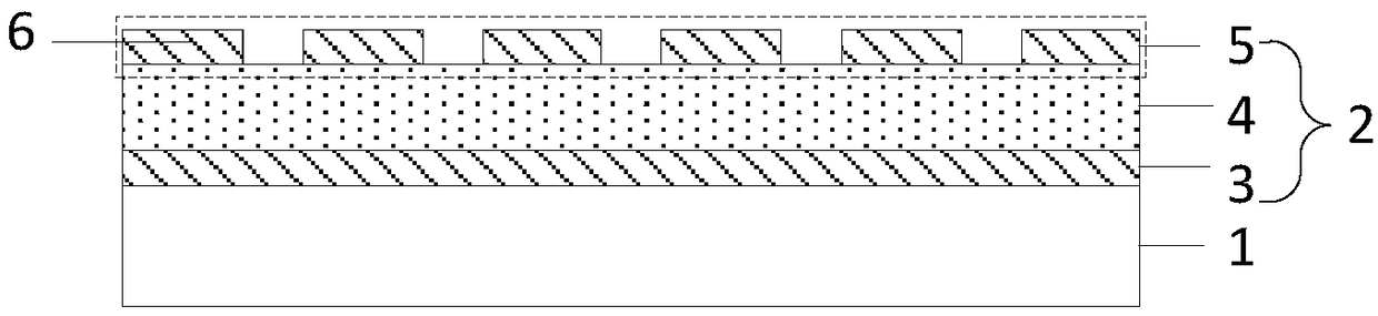
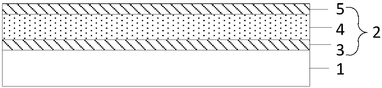
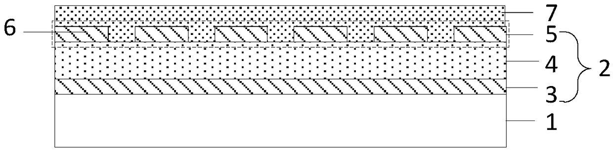
[0036] The embodiment of the present application provides a transfer substrate of a micro light emitting diode, such as figure 1 As shown, the transfer substrate includes: a first base substrate 1 and an electrostrictive layer 2 located on the first substrate substrate 1; the electrostrictive layer 2 is used to: make each transfer The thickness of the electro-deformable layer 2 in the area corresponding to the micro-light emitting diode is greater than the thickness of the electro-deformable layer 2 in the area corresponding to the micro-light-emitting diode that does not need to be transferred this time.

[0037]The transfer substrate of the micro-light-emitting diodes provided in the embodiment of the present application is equipped with an electro-deformable layer, and the height of the electro-deformable layer can be changed by applying power to the electro-deformable layer, so that the micro-light-emitting diodes that need to be transferred each time correspond to The thi...


PUM


Abstract

The invention discloses a micro light emitting diode transfer substrate and method, a display panel and a preparation method, and aims at simplifying the process complexity of micro light emitting diode preparation. The micro light emitting diode transfer substrate comprises a first substrate and an electrically induced deformation layer which is located on the first substrate, wherein the electrically induced deformation layer is used for ensuring that the thickness of the electrically induced deformation layer in a to-be-transferred area of a to-be-transferred micro light emitting diode is greater than the thickness of the electrically induced deformation layer in a not-to-be-transferred area corresponding to the micro light emitting diode.

Description

technical field [0001] The present application relates to the field of display technology, in particular to transfer substrates and transfer methods for micro-light emitting diodes, display panels and preparation methods. Background technique [0002] In recent years, research on the display of micro light-emitting diodes (Micro LEDs) has become a hot topic. Micro LED (Micro LED) is a device with a size between several microns and hundreds of microns. Because it is much smaller than ordinary LEDs, it is possible to use a single LED as a pixel (Pixel) for display. Micro An LED display is a display that uses a high-density Micro LED array as a display pixel array to display images. Each pixel can be addressed and driven to light up independently. It can be regarded as a reduced version of an outdoor LED display. Distances are reduced from millimeters to microns. At present, the Micro LED device needs to be grown on the supply substrate, and then the Micro LED is transferred ...

Claims


Application Information

Patent Timeline
Patent Type & Authority Applications(China)
IPC IPC(8): H01L33/00H01L33/48H01L27/15
CPCH01L27/156H01L33/0066H01L33/48H01L2933/0033H01L33/0093
Inventor 黄华赵承潭朱小研谢昌翰
Owner BOE TECH GRP CO LTD
Why Eureka
Try Eureka