Chip transfer method, chip and target substrate

A chip transfer and substrate technology, applied in semiconductor/solid-state device components, semiconductor devices, electrical components, etc., can solve the problems of low transfer efficiency of μTP technology and small number of Micro LED chips, and achieve batch transfer with high transfer efficiency Effect

Active Publication Date: 2021-05-14
BOE TECH GRP CO LTD
View PDF4 Cites 0 Cited by
  • Summary
  • Abstract
  • Description
  • Claims
  • Application Information

AI Technical Summary

Problems solved by technology

[0004] However, the number of Micro LED chips picked up each time by the elastic die is small, so the transfer efficiency of μTP technology is low

Method used


Image

  • Chip transfer method, chip and target substrate
  • Chip transfer method, chip and target substrate
  • Chip transfer method, chip and target substrate

Examples


Embodiment Construction

[0076] In order to make the purpose, technical solution and advantages of the application clearer, the application will be further described in detail below in conjunction with the accompanying drawings. Apparently, the described embodiments are only some of the embodiments of the application, not all of them. Based on the embodiments in this application, all other embodiments obtained by persons of ordinary skill in the art without making creative efforts belong to the scope of protection of this application.

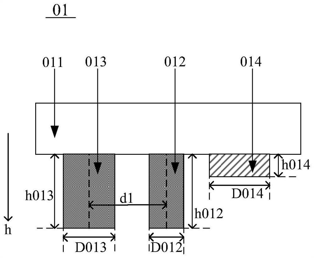
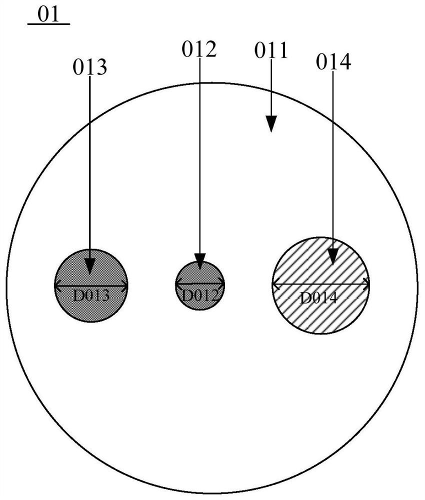
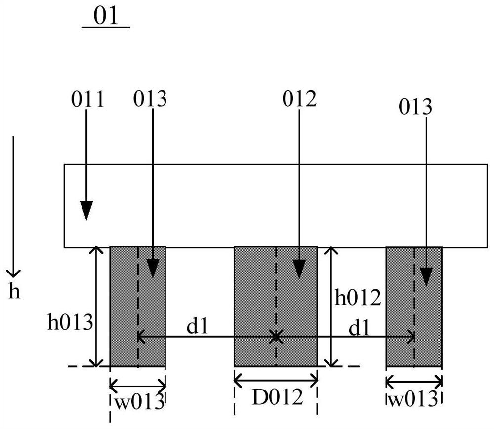
[0077] Micro LED technology is a new type of display technology that can be better applied to display products such as TVs, iPhones (Apple mobile phones) and iPads (Apple tablet computers). Micro LED chip is a kind of nanoscale LED chip. Micro LED chip usually needs to be formed by molecular beam epitaxy on sapphire substrate (hereinafter referred to as source substrate). The size of sapphire substrate is usually the size of silicon wafer. Smaller, and the size of the ...


PUM


Abstract

The application discloses a chip transfer method, a chip and a target substrate, belonging to the field of chip transfer. The method includes: setting the target substrate in a closed chamber, and applying charges of the first polarity to the first substrate bonding structure of the target substrate; applying charges of the second polarity to the first chip bonding structure of the chip, the second The second polarity is different from the first polarity; the insulating fluid is injected into the sealed chamber to suspend the chip in the insulating fluid, and the first chip bonding structure moves close to the first substrate bonding structure, driving the chip to move close to the target substrate, the first The chip bonding structure is in contact with the first substrate bonding structure through the alignment hole, and the second chip bonding structure is in contact with the second substrate bonding structure through the alignment seam; pressure is applied to the chip so that the first chip bonding structure is in contact with the second substrate bonding structure. A substrate bonding structure is bonded, and a second chip bonding structure is bonded to the second substrate bonding structure. The application can improve the transfer efficiency of the chip. This application is for chip transfer.

Description

technical field [0001] The present application relates to the field of chip transfer, in particular to a chip transfer method, chip and target substrate. Background technique [0002] Micro Light Emitting Diode (English: Micro Light Emitting Diode; abbreviation: Micro LED / μLED) chip is a new type of LED chip, which has the advantages of high brightness, high luminous efficiency and low power consumption, and has broad application prospects in the display industry. Micro LED chips usually need to be formed on a sapphire substrate (hereinafter referred to as the source substrate), and the Micro LED chip needs to be transferred from the source substrate to the target substrate (such as a display backplane) during use. [0003] At present, Micro LED chips are mainly transferred by micro transfer printing (English: Micro Transfer Printing; abbreviation: μTP) technology. The transfer equipment used in μTP technology includes a print head and an elastic stamp (English: stamp). The...

Claims


Application Information

Patent Timeline
Patent Type & Authority Patents(China)
IPC IPC(8): H01L21/683H01L21/68H01L33/62
CPCH01L21/6835H01L21/68H01L33/62H01L2933/0066H01L2221/68363H01L23/544H01L2223/54426H01L2223/54486H01L2221/68322H01L2221/68354H01L2224/81191H01L2224/1403H01L2224/13H01L24/06H01L24/14H01L24/16H01L24/17H01L24/81H01L25/167H01L2224/06051H01L2224/14051H01L2224/16145H01L2224/1703H01L2224/17051H01L2224/81085H01L2224/81139H01L2224/81143
Inventor 陈亮王磊玄明花肖丽刘冬妮赵德涛陈昊
Owner BOE TECH GRP CO LTD
Why Eureka
Try Eureka