Chip, target substrate, chip transfer method and display device

A display device and chip technology, applied in semiconductor/solid-state device components, semiconductor devices, electrical components, etc., can solve the problem of low transfer efficiency of μTP technology

Active Publication Date: 2020-04-17
BOE TECH GRP CO LTD
View PDF3 Cites 0 Cited by
  • Summary
  • Abstract
  • Description
  • Claims
  • Application Information

AI Technical Summary

Problems solved by technology

However, in μTP technology, the number of MicroLED chips picked up each time by the elastic die is small, so the transfer efficiency of μTP technology is low

Method used


Image

  • Chip, target substrate, chip transfer method and display device
  • Chip, target substrate, chip transfer method and display device
  • Chip, target substrate, chip transfer method and display device

Examples


Embodiment Construction

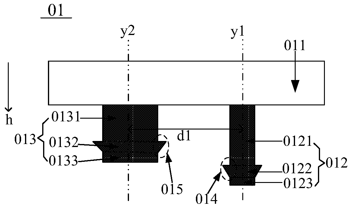
[0008] Please refer to figure 1 , which shows a schematic structural diagram of a chip 01 provided in an embodiment of the present application. The chip 01 includes a chip body 011 and a first chip bonding structure 012 and a second chip bonding structure 013 arranged on the chip body 011. The first chip bonding structure 012 and the second chip bonding structure 013 are located on the same side of the chip body 011, and the first chip bonding structure 012 and the second chip bonding structure 013 are arranged on the same layer, and the first chip bonding structure 012 The side surface of the second chip bonding structure 013 has a first chip engaging portion 014 , and the side surface of the second chip bonding structure 013 has a second chip engaging portion 015 . The first die bonding structure 012 is configured to pass through the target substrate ( figure 1 Not shown in the first alignment hole ( figure 1 Not shown in ) and the first substrate bonding structure of the ...


PUM


Abstract

A chip, a target substrate, a chip transfer method and a display device, belonging to the field of chip transfer. The transfer method includes: setting the target substrate in a closed chamber; applying charges of different polarities to the first chip bonding structure and the first substrate bonding structure, injecting insulating fluid into the closed chamber and controlling the first substrate bonding structure Potential, make the first chip bonding structure enter the first alignment hole and be located between the first substrate clamping part and the first substrate bonding structure; apply different poles to the second chip bonding structure and the second substrate bonding structure The electric charge changes the flow direction of the insulating fluid and controls the potential of the second substrate bonding structure, so that the second chip bonding structure enters the second alignment hole and is located between the second substrate clamping part and the second substrate bonding structure Between; apply pressure to the chip to bond the chip bonding structure with the substrate bonding structure. The application can improve chip transfer efficiency.

Description

technical field [0001] The present application relates to the field of chip transfer, in particular to a chip, a target substrate, a chip transfer method and a display device. Background technique [0002] Micro Light Emitting Diode (Micro LED / μLED) chip is a new type of LED chip, which has the advantages of high brightness, high luminous efficiency and low power consumption, and has broad application prospects in the display industry. Micro LED chips usually need to be formed on a sapphire substrate (hereinafter referred to as the source substrate), and the Micro LED chip needs to be transferred from the source substrate to the target substrate during use. At present, Micro LED chips are mainly transferred by Micro Transfer Printing (μTP) technology. However, in μTP technology, the number of MicroLED chips picked up each time by the elastic stamper is small, so the transfer efficiency of μTP technology is low. Contents of the invention [0003] The present application p...

Claims


Application Information

Patent Timeline
Patent Type & Authority Patents(China)
IPC IPC(8): H01L33/00H01L23/488H01L21/60
CPCH01L24/81H01L24/14H01L33/0095H01L2224/81143H01L2224/81236H01L2224/14051H01L2224/1403H01L2224/14517H01L2224/81897H01L2933/0066H01L33/005H01L33/20
Inventor 陈亮王磊玄明花刘冬妮肖丽赵德涛陈昊
Owner BOE TECH GRP CO LTD
Why Eureka
Try Eureka