Method and sample holder for the controlled bonding of substrates
A technology of substrate and contact surface, applied in semiconductor/solid-state device manufacturing, electrical components, circuits, etc., can solve problems such as error-proneness, high cost, and low output, and achieve the effect of reducing distortion
- Summary
- Abstract
- Description
- Claims
- Application Information
AI Technical Summary
Problems solved by technology
Method used
Image

Examples
Embodiment Construction
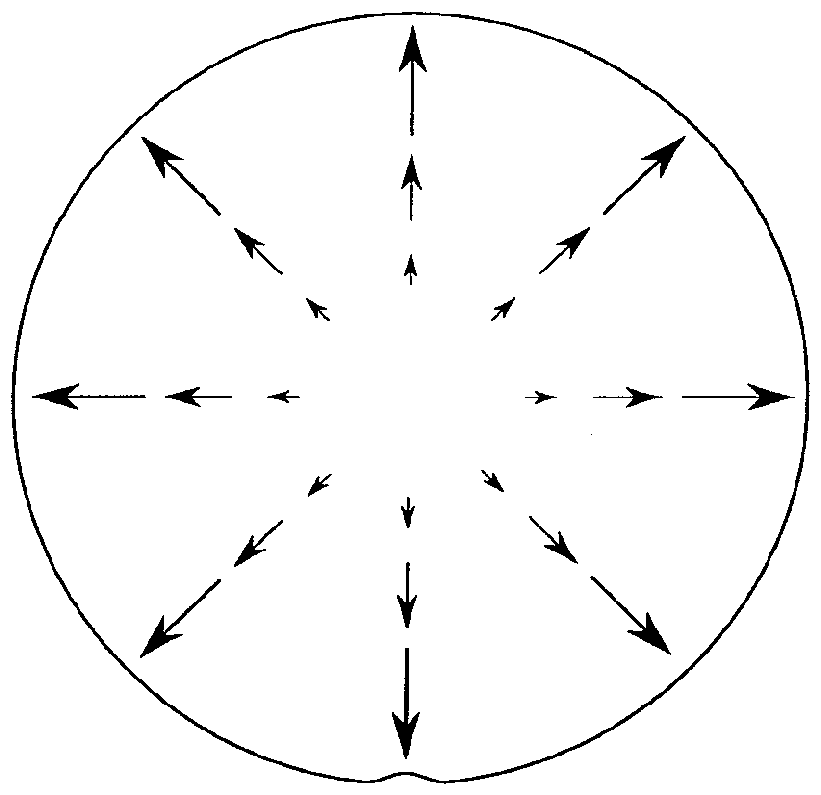
[0227] The X-axis runs in the receiving surface 1s, 1s', 1s", 1s'" of the substrate holder 1o or 1u. The Y-axis runs perpendicular to the X-axis and likewise in the receiving surface 1s, 1s of the substrate holder 1o or 1u ', 1s", 1s''' extended. The Z-axis extends perpendicularly to the X-axis and the Y-axis and perpendicularly to the receiving surfaces 1s, 1s', 1s", 1s''' of the substrate holder 1o or 1u.
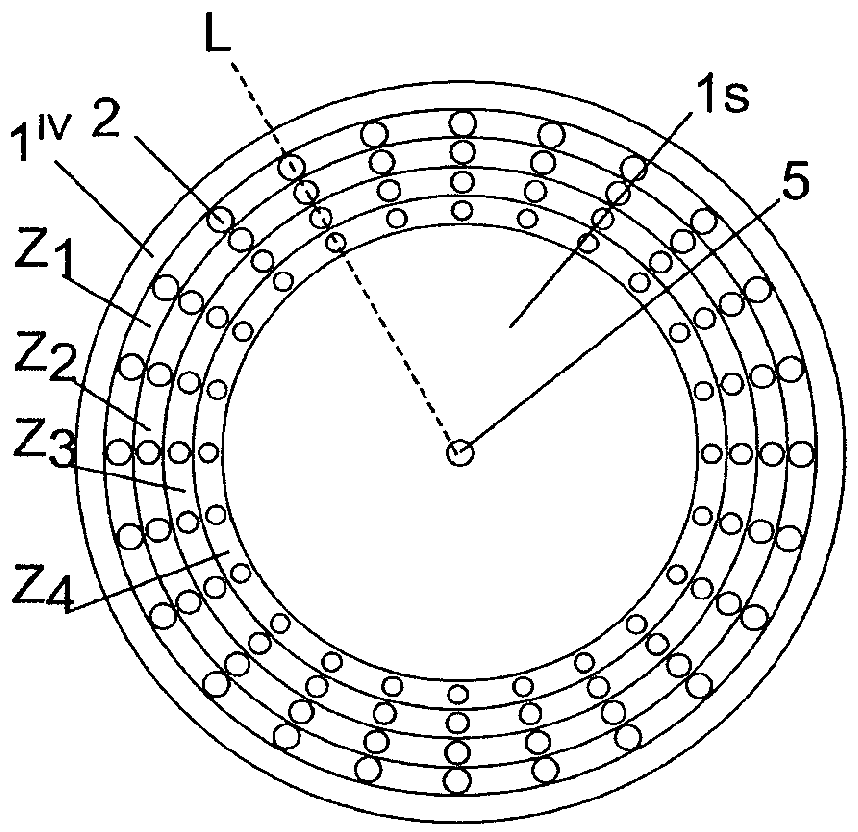
[0228] 1 a shows a schematic, not to scale partial view of a cross-section of a first embodiment of a holding device 1 according to the invention (alternatively referred to as a substrate holder), wherein only the fastening elements 2 are shown. (Fixing device) edge region R.
[0229] The receiving device 1 is composed of a plurality of zones Zi, which are preferably located in the edge region R. As shown in FIG. Each of the zones Zi can have a plurality of fixation elements 2 . Two zones Z1 and Z2 are shown by way of example in FIG. 1a. Four fastening elements 2 are ...
PUM
 Abstract
Description
Claims
Application Information
 - R&D
- Intellectual Property
- Life Sciences
- Materials
- Tech Scout
- Unparalleled Data Quality
- Higher Quality Content
- 60% Fewer Hallucinations
Browse by: Latest US Patents, China's latest patents, Technical Efficacy Thesaurus, Application Domain, Technology Topic, Popular Technical Reports.
© 2025 PatSnap. All rights reserved.Legal|Privacy policy|Modern Slavery Act Transparency Statement|Sitemap|About US| Contact US: help@patsnap.com