Circuit board with stepped pad, and moulding method thereof

A molding method and stepped technology, applied in the direction of printed circuits, printed circuits, printed circuit components, etc., can solve the problems of increased wiring density, achieve effective heat dissipation, solve the increased wiring density, and ensure the effect of performance

Active Publication Date: 2019-03-29
GUANGZHOU FASTPRINT CIRCUIT TECH +1
View PDF7 Cites 0 Cited by
  • Summary
  • Abstract
  • Description
  • Claims
  • Application Information

AI Technical Summary

Problems solved by technology

[0003] Based on this, it is necessary to provide a circuit board with stepped pads and its forming method for the current problem of increased wiring density due to increased functional requirements.

Method used


Image

  • Circuit board with stepped pad, and moulding method thereof
  • Circuit board with stepped pad, and moulding method thereof
  • Circuit board with stepped pad, and moulding method thereof

Examples


Embodiment Construction

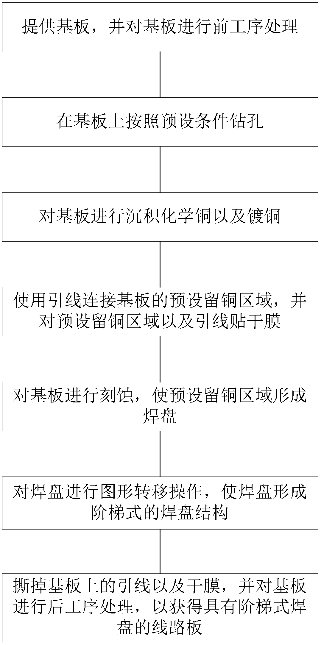
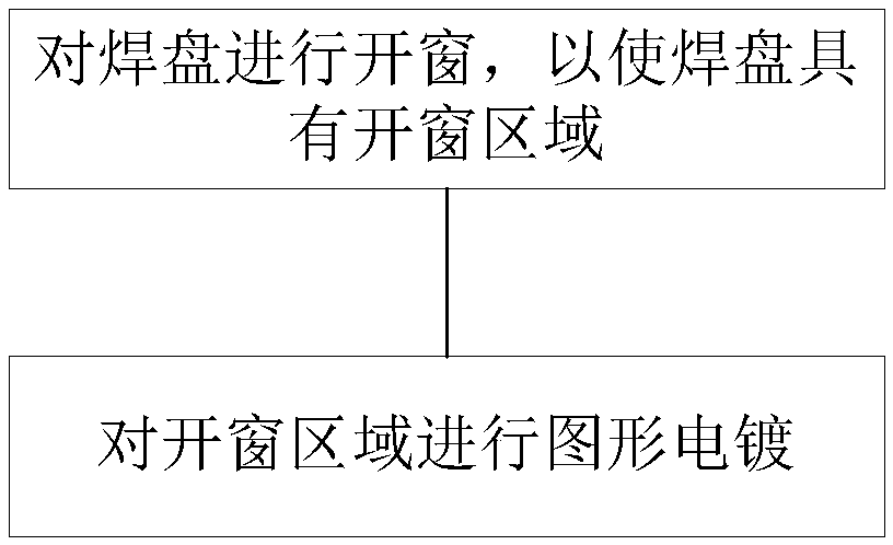
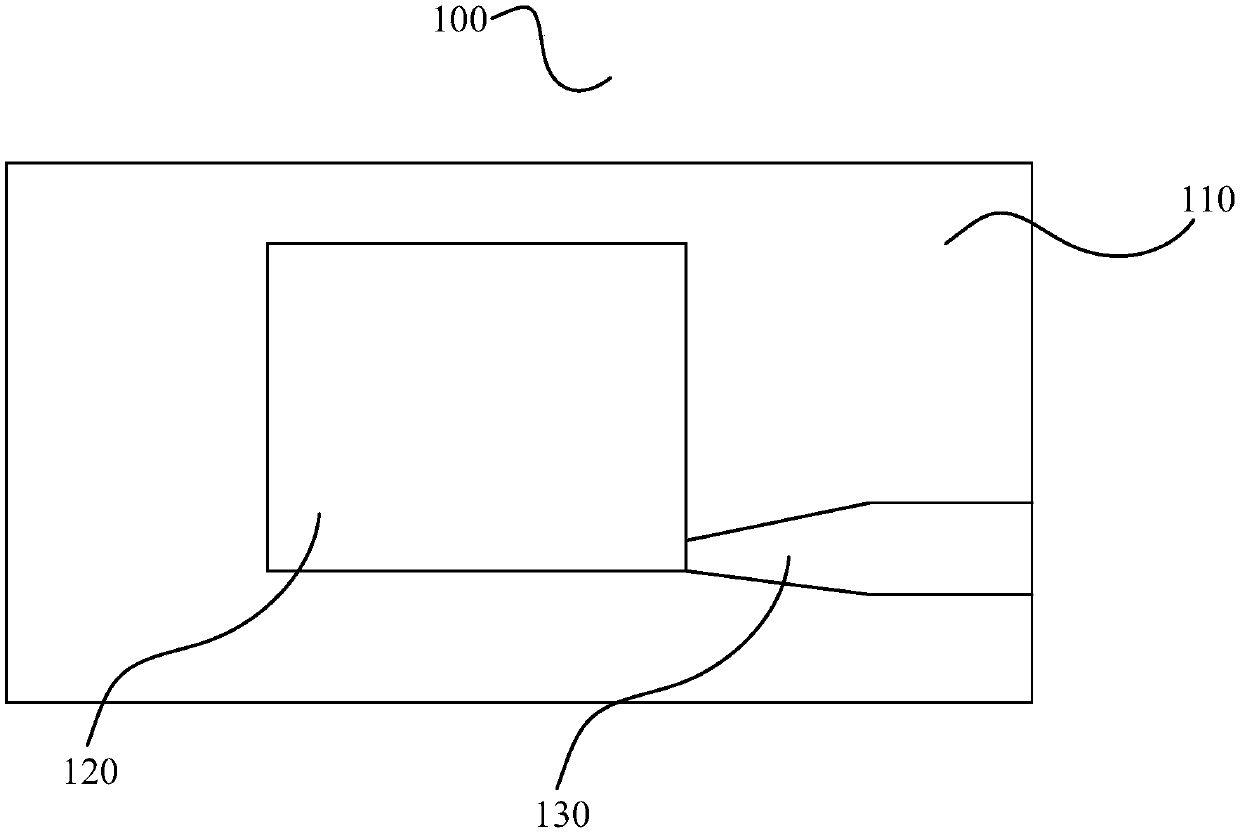
[0041] In order to make the purpose, technical solution and advantages of the present invention clearer, the circuit board with stepped pads and its forming method of the present invention will be further described in detail through the following embodiments and in conjunction with the accompanying drawings. It should be understood that the specific embodiments described here are only used to explain the present invention, not to limit the present invention.

[0042] The serial numbers assigned to components in this document, such as "first", "second", etc., are only used to distinguish the described objects, and do not have any sequence or technical meaning. The "connection" and "connection" mentioned in this application all include direct and indirect connection (connection) unless otherwise specified. In describing the present invention, it is to be understood that the terms "upper", "lower", "front", "rear", "left", "right", "vertical", "horizontal", "top", The orientatio...


PUM

PropertyMeasurementUnit
thicknessaaaaaaaaaa

Abstract

The invention provides a circuit board with a stepped pad, and a moulding method thereof. The moulding method of the circuit board with a stepped pad includes the following steps: providing a base material; according to preset conditions, drilling the base material; performing deposition of chemical copper and copper facing on the base material; connecting a preset copper-remaining region of the base material by means of a lead wire, and sticking a dry film to the preset copper-remaining region and the lead wire; etching the base material to enable the preset copper-remaining region to form apad; performing pattern transfer operation on the pad to enable the pad to form a stepped pad structure; and tearing off the lead wire on the base material and the dry film, performing post-process processing on the base material to obtain a circuit board with a stepped pad. The stepped pad structure can increase the function demand while enabling wiring to be dispersed to enable a heat radiationgradient on the circuit board to satisfy the application requirement of the user for multifunction of the circuit board.

Description

technical field [0001] The invention relates to the technical field of PCB, in particular to a circuit board with stepped pads and a forming method thereof. Background technique [0002] With the rapid development of the circuit board industry, in order to increase the diversification of circuit board function requirements, or to meet the special needs of customers, it is necessary to add corresponding pads on the circuit board. However, this will increase the wiring density of the circuit board, resulting in uneven heat dissipation of the circuit board and affecting the performance of the circuit board. Contents of the invention [0003] Based on this, it is necessary to provide a circuit board with stepped pads and a forming method thereof for the current problem of increased wiring density due to increased functional requirements. [0004] Above-mentioned purpose realizes through following technical scheme: [0005] A method for forming a circuit board with stepped pa...

Claims


Application Information

Patent Timeline
Patent Type & Authority Applications(China)
IPC IPC(8): H05K3/40H05K1/11
CPCH05K1/116H05K3/40H05K2201/09845
Inventor 许龙龙罗畅陈黎阳
Owner GUANGZHOU FASTPRINT CIRCUIT TECH
Why Eureka
Try Eureka