Mixing and stirring integrated facility for producing and processing semi-conductive materials

A semi-conductive and facility technology, which is applied in the field of mixing and stirring integrated facilities, can solve the problems of poor defoaming effect, many bubbles, and poor heating and mixing effect of semi-conductive raw materials, so as to ensure the effect of later use, ensure the quality of mixing, and improve The effect of mixing effects

Inactive Publication Date: 2019-04-12
宁波华越高分子科技有限公司
View PDF9 Cites 1 Cited by
  • Summary
  • Abstract
  • Description
  • Claims
  • Application Information

AI Technical Summary

Problems solved by technology

[0005] In order to solve the above-mentioned technical problems, the present invention provides an integrated mixing and stirring facility for the production and processing of semiconductive materials to solve the problem of the existing similar facilities, which have poor heating and mixing effects on granular semiconductive raw materials, and the semiconductive raw materials are prone to contain Unevenness occurs, which affects the mixing effect of semi-conductive materials; and the effect of defoaming inside semi-conductive raw materials is poor, and semi-conductive raw materials after mixing and stirring tend to contain more bubbles inside, which affects the use effect of semi-conductive materials

Method used


Image

  • Mixing and stirring integrated facility for producing and processing semi-conductive materials
  • Mixing and stirring integrated facility for producing and processing semi-conductive materials
  • Mixing and stirring integrated facility for producing and processing semi-conductive materials

Examples


Embodiment

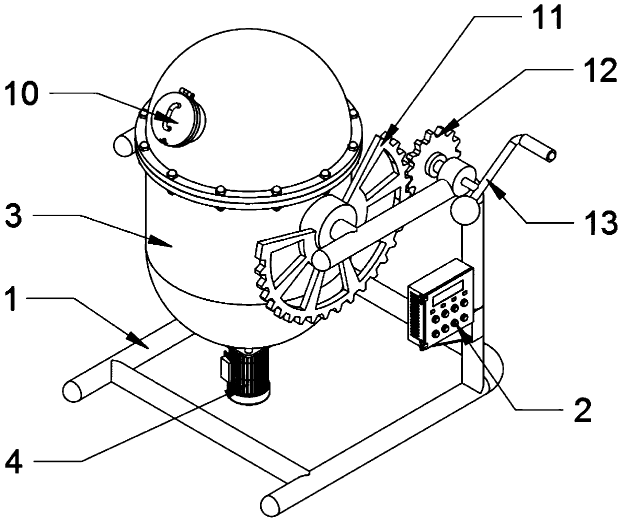
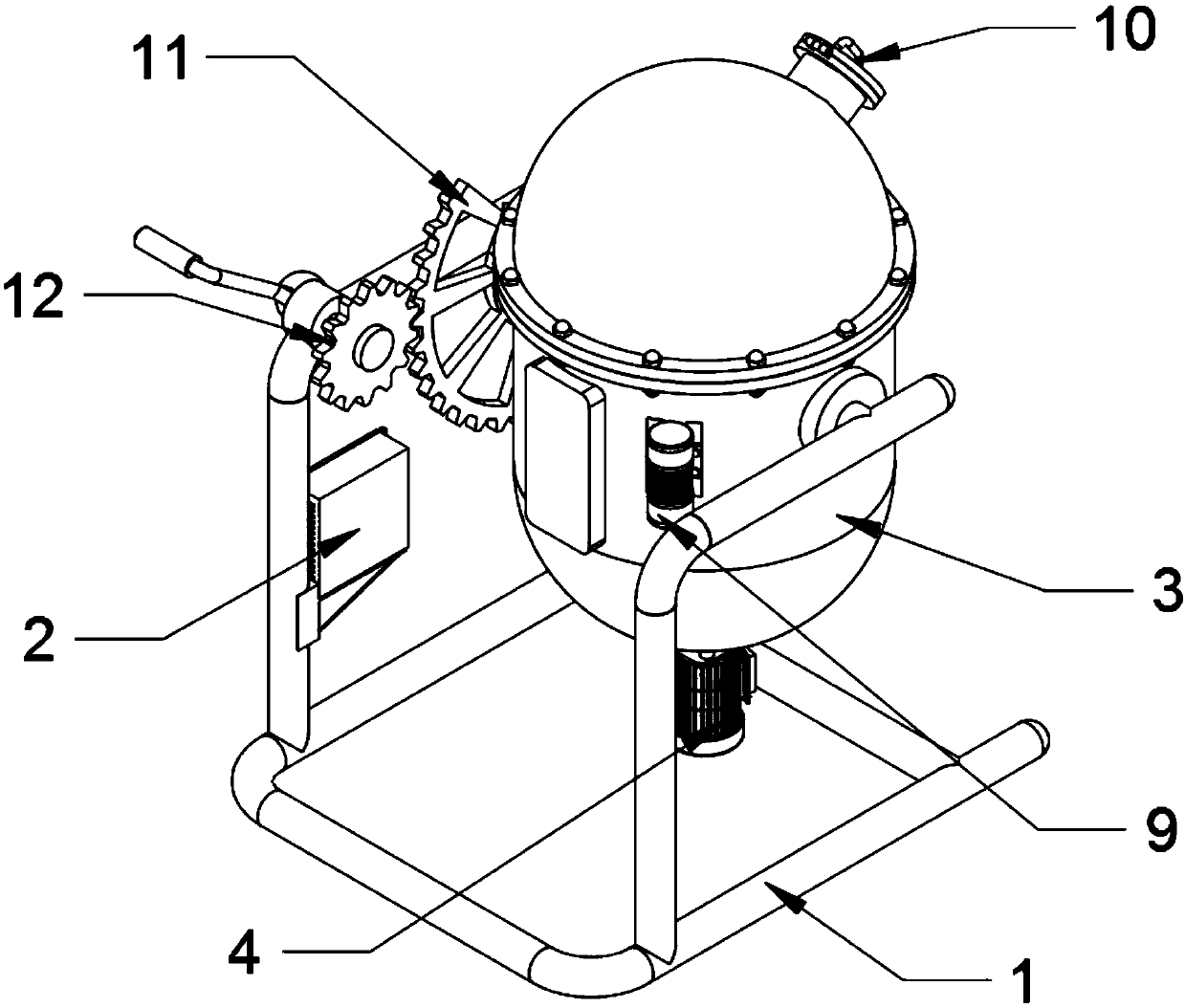
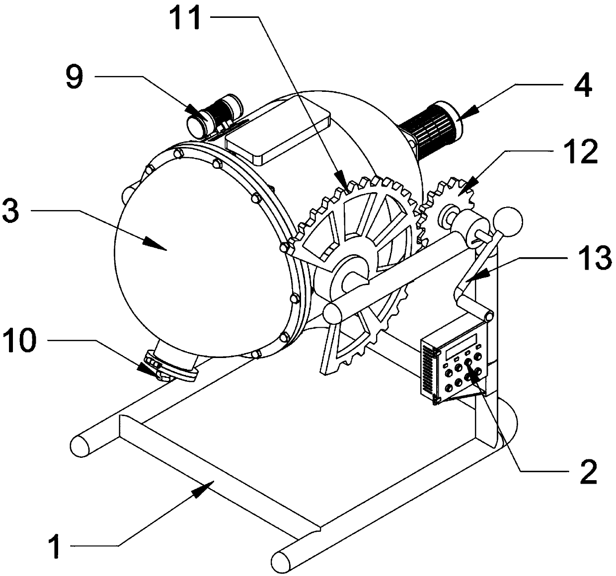
[0031] as attached figure 1 to attach Figure 8 Shown:

[0032] The invention provides an integrated mixing and stirring facility for the production and processing of semi-conductive materials, including a support base 1, a power control box 2, a mixing tank 3, a feeding port 301, a stirring motor 4, a mixing shaft 5, and a stirring frame 6 , stirring blade 7, heating ring 8, vibration motor 9, sealing cover 10, driven wheel 11, driving wheel 12 and manual crank 13; the power control box 2 is installed on the right side of the support base 1, and the support base 1 is a frame structure, and the mixing tank 3 is installed in the top of the support seat 1; the inside of the mixing tank 3 is a hollow structure, and the top of the mixing tank 3 is provided with a feeding port 301; the stirring motor 4 is installed in the mixing tank 3 on the bottom end face, and the stirring motor 4 is electrically connected to the power control box 2 through the power line; the bottom of the mi...


PUM


Abstract

The invention provides a mixing and stirring integrated facility for producing and processing semi-conductive materials. The facility comprises a driving wheel and a manual rocking handle; a power supply control box is mounted on the right side of a support base, the support base is of a frame structure, and a mixing barrel is mounted in the top of the support base; the interior of the mixing barrel is of a hollow structure, and the top of the mixing barrel is provided with a feed inlet; a stirring motor is mounted on the end face of the bottom of the mixing barrel and electrically connected with the power control box through a power supply circuit; the bottom of a mixing shaft is connected with the top of the stirring motor, and the mixing shaft rotates in the mixing barrel; the stirringframe is mounted on the mixing shaft, and stirring blades are mounted on the stirring frame; a heating ring is mounted in the mixing barrel, and a vibration motor is mounted outside the mixing barrel.The facility is beneficial to mixing and stirring of the semi-conductive raw materials contained in a device, so that the semi-conductive raw materials are mixed more uniformly, and the mixing quality of the semi-conductive materials is ensured.

Description

technical field [0001] The invention belongs to the technical field of production and processing of semiconductive materials, and more specifically relates to an integrated mixing and stirring facility for production and processing of semiconductive materials. Background technique [0002] Semi-conductive composite materials are widely used in high-voltage cables, for example, between the conductor and the insulating layer to uniform the electric field. Especially in high-voltage DC cables, due to the accumulation of space charges in the insulating layer, it is easy to cause electric field distortion, resulting in accelerated aging and even breakdown. A large number of studies have shown that the charge in the cable insulation layer is not only derived from the metal core, but also closely related to the charge emission of the semiconductive composite material. [0003] The inventors found that there are existing similar mixing and stirring integrated facilities for the pro...

Claims


Application Information

Patent Timeline
Patent Type & Authority Applications(China)
IPC IPC(8): B01F7/32B01F15/02B01F15/06B01F27/96
CPCB01F27/96B01F35/7548B01F35/92B01F2101/58
Inventor 岑哲君
Owner 宁波华越高分子科技有限公司
Why Eureka
Try Eureka