AI technical title is built by Patsnap AI team. It summarizes the technical point description of the patent document.
A technology of transmission lines and waveguides, used in circuits, waveguides, electrical components, etc.
Inactive Publication Date: 2021-02-23
FUJIKURA LTD
View PDF11 Cites 0 Cited by
Summary
Abstract
Description
Claims
Application Information
AI Technical Summary
This helps you quickly interpret patents by identifying the three key elements:
Problems solved by technology
Method used
Benefits of technology
Problems solved by technology
When the dielectric substrate constituting the columnar waveguide is formed of a brittle material such as glass, there is a problem in terms of strength
Method used
Image
Click on the blue label to locate the original text in one second.
Reading with bidirectional positioning of images and text.
Examples
Embodiment 1
[0102] The inventors of the present application actually designed and simulated the transmission line of the above-mentioned first embodiment, and obtained the intensity distribution of a high-frequency signal transmitted through the transmission line, and the reflection characteristics and transmission characteristics of the transmission line. Design parameters of the transmission line 1 for simulation are as follows.
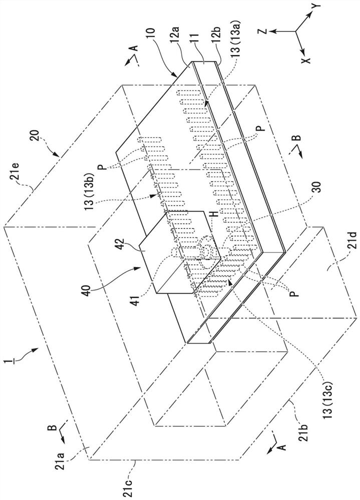
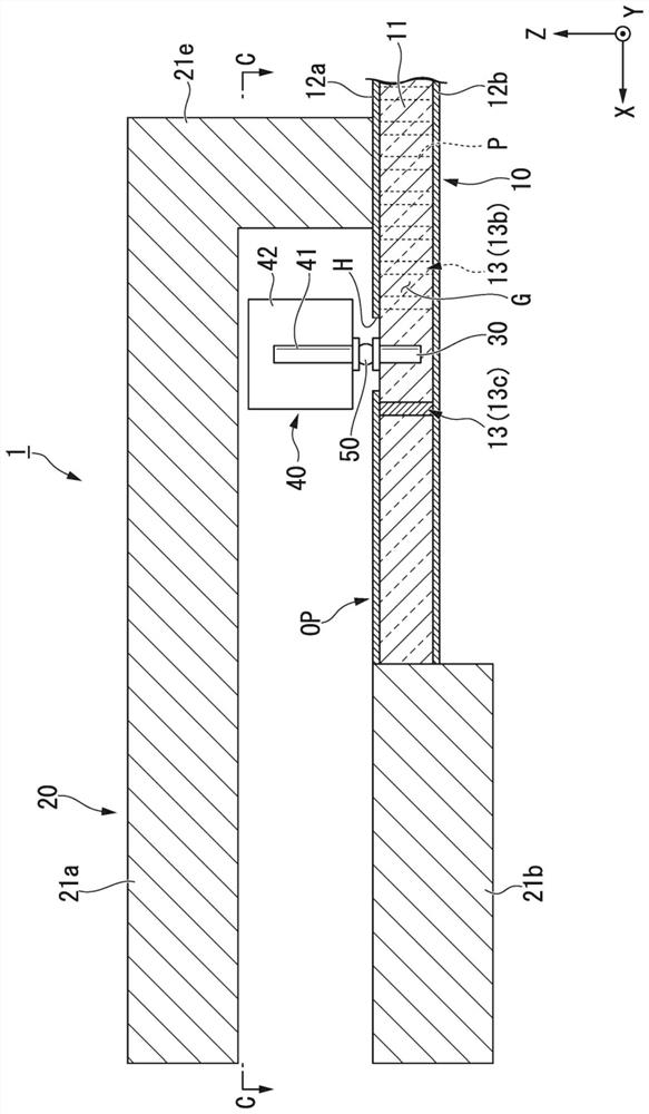
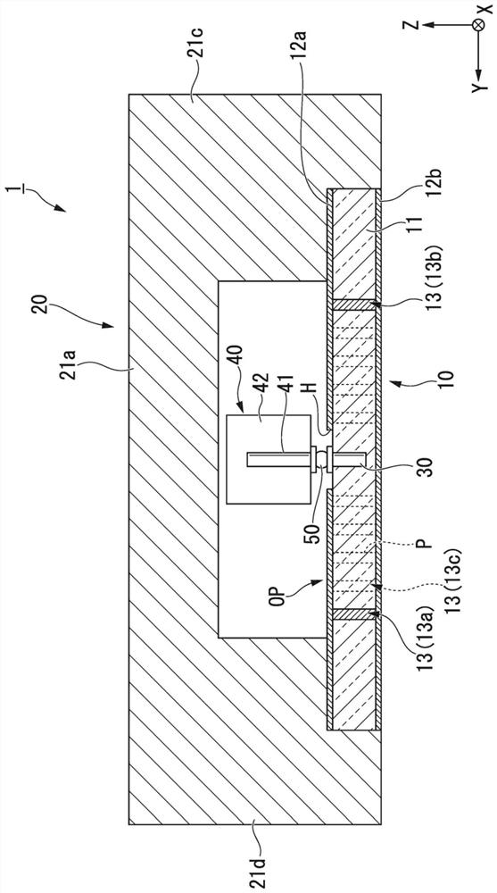
[0103] ·Pillar wall waveguide 10
[0104] Thickness of dielectric substrate 11: 520 [μm]
[0105] Relative permittivity of dielectric substrate 11: 3.82
[0106] Interval between the first column walls 13a, 13b (distance between centers): 1540 [μm]
[0107] The distance between the second column wall 13c and the blind hole 30 (center-to-center distance): 480 [μm]
[0108] Diameter of opening H (isolating disk AP): 340 [μm]
[0109] ·Waveguide 20
[0110] Height inside the tube: 1149[μm]
[0111] Width inside the tube: 2500[μm]
[0112] Distance from the...
Embodiment 2
[0131] In addition, the inventors of the present application actually designed the transmission line of the above-mentioned second embodiment, performed simulations, and obtained the reflection characteristics of the transmission line. Design parameters of the transmission line 1 for simulation are as follows.
[0132] ·Column wall waveguide 60
[0133] Thickness of dielectric substrate 11: 520 [μm]
[0134] Relative permittivity of dielectric substrate 11: 3.82
[0135] Interval between the first column walls 63a, 63b (distance between centers): 1540 [μm]
[0136] The distance between the second column wall 63c and the blind hole 30 (center-to-center distance): 480 [μm]
[0137] Diameter of opening H (isolating disk AP): 340 [μm]
[0138] ·Waveguide 20
[0139] Height inside the tube: 1149[μm]
[0140] Width inside the tube: 2500[μm]
[0141]Distance from the center of conductor post 41 to narrow wall 21e: 985 [μm]
[0142] Outer diameter of conductor post P: 100 [μm]...
PUM
Property
Measurement
Unit
relative permittivity
aaaaa
aaaaa
Abstract
The transmission line has: a pillar wall waveguide having a dielectric substrate on which a pair of pillar walls are formed, and a first conductor layer and a second conductor layer opposed to each other via the dielectric substrate. The area surrounded by the wall, the first conductor layer, and the second conductor layer is a waveguide area; a hollow square waveguide, the waveguide is connected to the opening formed on the side wall in such a way that the first conductor layer covers The first conductor layer is connected, the inside of the waveguide is connected to the waveguide region through the opening formed in the first conductor layer; the blind hole is formed in such a way that one end of the blind hole is arranged inside the opening on the dielectric substrate; and a rod part having a post part connected to the one end of the blind hole and a support part supporting the post part, the post part is connected to the blind hole by the post part. The holes are coaxially arranged in the waveguide.
Description
technical field [0001] The present invention relates to transmission lines. [0002] This application claims priority based on Japanese application No. 2016-165770 filed in Japan on August 26, 2016, and the content is cited here. Background technique [0003] Conventionally, waveguides have been used as transmission lines for transmitting high-frequency signals from the microwave band (0.3 to 30 [GHz]) to the millimeter wave band (30 to 300 [GHz]). In addition, in recent years, a post-wall waveguide (PWW: Post-Wall Wave guide) has also been used as a transmission line for transmitting such a high-frequency signal. The pillar wall waveguide is a square waveguide formed by a pair of conductor layers and a pair of pillar walls. The pair of conductor layers are formed on both sides of the dielectric substrate. Conductor posts are arranged in two rows. [0004] The above-mentioned waveguide and column wall waveguide may be used alone or in combination. For example, in a commu...
Claims
Application Information
Patent Timeline
Application Date:The date an application was filed.
Publication Date:The date a patent or application was officially published.
First Publication Date:The earliest publication date of a patent with the same application number.
Issue Date:Publication date of the patent grant document.
PCT Entry Date:The Entry date of PCT National Phase.
Estimated Expiry Date:The statutory expiry date of a patent right according to the Patent Law, and it is the longest term of protection that the patent right can achieve without the termination of the patent right due to other reasons(Term extension factor has been taken into account ).
Invalid Date:Actual expiry date is based on effective date or publication date of legal transaction data of invalid patent.

