Photonic crystal device

a technology of photonic crystal and optical coupling, which is applied in the direction of optical waveguide light guide, instruments, nanotechnology, etc., can solve the problems of difficult to realize a precise adjustment of the degree of optical coupling, and it is impossible to achieve a design which simultaneously realizes desired values, so as to achieve the effect of improving accuracy

Active Publication Date: 2006-02-16
PANASONIC CORP
View PDF10 Cites 20 Cited by
  • Summary
  • Abstract
  • Description
  • Claims
  • Application Information

AI Technical Summary

Benefits of technology

[0014] In order to overcome the problems described above, preferred embodiments of the present invention provide a photonic crystal device which is capable of realizing, with an improved accuracy, an adjustment of the matching between an optical waveguide and an optical resonator.
[0025] In accordance with a photonic crystal structure of the present invention, the degree of coupling between the optical resonator and the optical waveguide is adjusted by adjusting the depths of holes, rather than based on presence / absence of defects in the photonic crystal or shifting of hole positions. As a result, there is provided an increased freedom of adjustment, and it is possible to realize a very small sized optical device which has a low light reflection loss. By applying the photonic crystal device of the present invention to an optical device such as an optical modulator, it becomes possible to reduce the size and enhance the performance of the device.

Problems solved by technology

However, this distance is set to be an integer multiple of the pitch of the air holes (lattice constant), and therefore it is difficult to realize a precise adjustment of the degree of optical coupling.
Therefore, it has been impossible to arrive at a design which simultaneously realizes desired values for the Q value, matching, and resonant frequency of the optical resonator.

Method used


Image

  • Photonic crystal device
  • Photonic crystal device
  • Photonic crystal device

Examples


embodiment 1

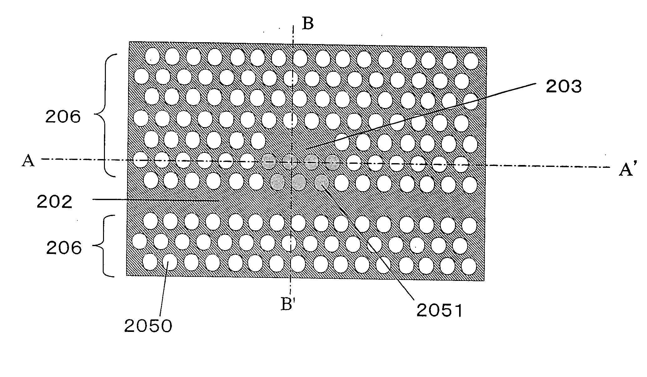
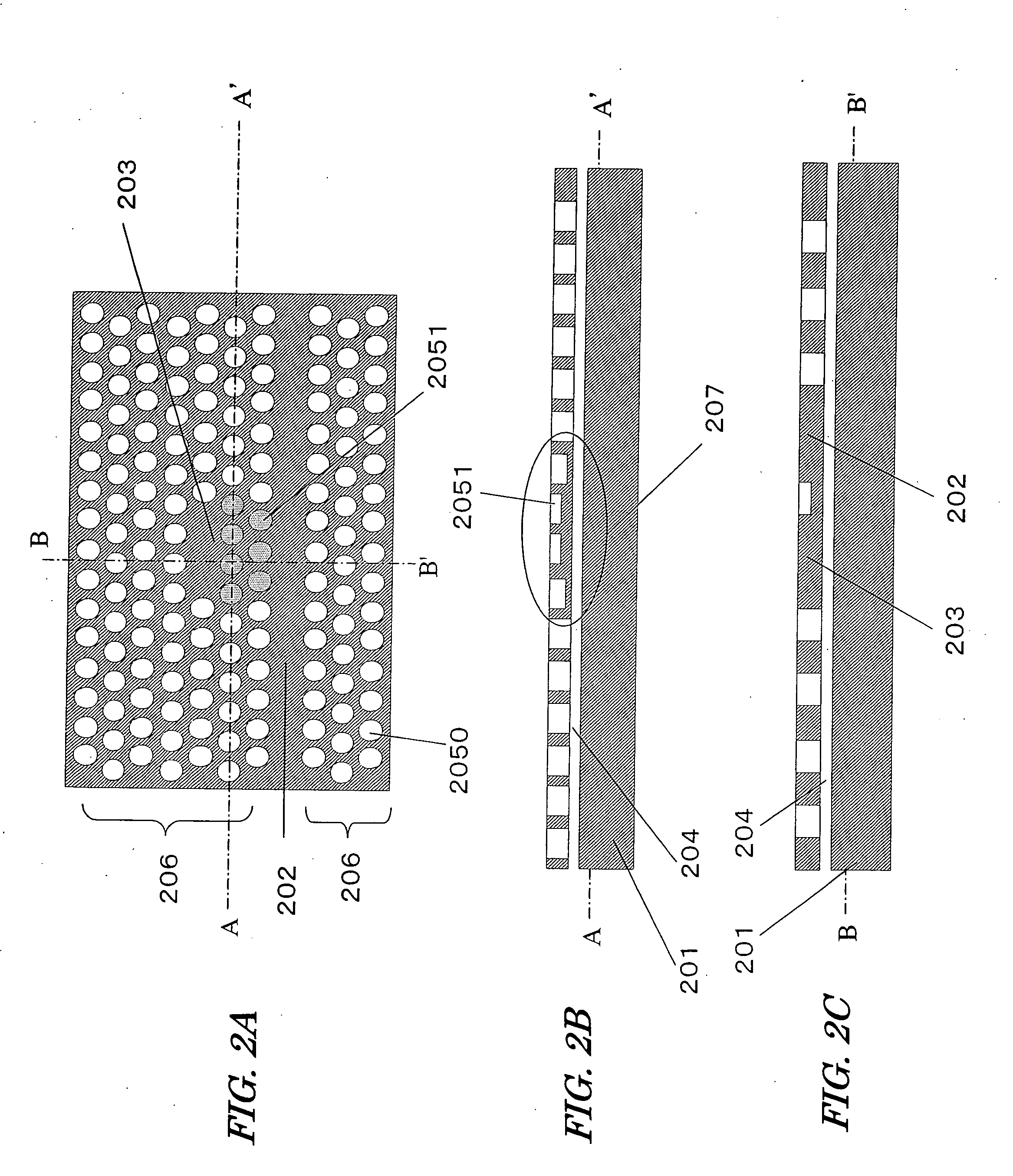
[0038] With reference to FIGS. 2A to 2C, a photonic crystal device according to a first embodiment of the present invention will be described. FIG. 2A is a view showing an upper face of the photonic crystal device of the present embodiment. FIG. 2B is a cross-sectional view taken at line A-A′ in FIG. 2A. FIG. 2C is a cross-sectional view taken at line B-B′ in FIG. 2A.

[0039] The photonic crystal device of the present embodiment includes: a substrate 201; a periodic structure portion 206 which is formed on the substrate 201; an optical waveguide 202 which is disposed adjacent to the periodic structure portion 206; and an optical resonator 203 which is formed in a position away from the optical waveguide 202. The periodic structure portion 206 has a plurality of holes 2050 which are arranged in a two-dimensional and periodic manner along a principal face of the substrate 201. The optical resonator 203 is formed in a position away from the optical waveguide 202, with at least one hole ...

embodiment 2

[0071] Hereinafter, with reference to FIGS. 4A to 4D, photonic crystal devices according to a second embodiment of the present invention will be described. Embodiment 1 illustrates a photonic crystal device in which an optical resonator is provided in a position away from the optical waveguide. In a photonic crystal device of the present embodiment, an optical resonator is provided within the optical waveguide. An optical resonator which is provided within an optical waveguide will hereinafter be referred to as an “optical waveguide type resonator”.

[0072] A photonic crystal device shown in FIG. 4A comprises: a substrate 201; a periodic structure portion 206 composed of holes 2050 periodically arrayed on the substrate 201; and an optical waveguide 202 provided on the substrate 201. The present embodiment is characterized in that, as shown in FIG. 4B, four holes 2051 are provided at an intermediate position in the optical waveguide 202, thus creating an optical resonator 203 in an in...

embodiment 3

[0074] Next, with reference to FIGS. 5A to 5D, photonic crystal devices according to a third embodiment of the present invention will be described.

[0075] In a photonic crystal device shown in FIGS. 5A and 5B, two holes 2051 are provided at a bent portion of an optical waveguide 202. On the other hand, in a photonic crystal device shown in FIGS. 5C and 5D, four holes 2051 are provided at a bent portion of an optical waveguide 202. In either photonic crystal device, the holes 2051 are made shallower than holes 2050 in a periodic structure portion 206. By adjusting the depth of the holes 2051, fine adjustment of the equivalent refractive index is realized. In the present embodiment, by adjusting the depth of the holes 2051, the transmission characteristics of the optical waveguide 202 are controlled.


PUM

PropertyMeasurementUnit
refractive indexaaaaaaaaaa
thicknessaaaaaaaaaa
thicknessaaaaaaaaaa

Abstract

A photonic crystal device according to the present invention includes: a substrate 201; a periodic structure portion 206 formed in or on the substrate 201, the periodic structure portion 206 having a plurality of holes 2050 and 2051 arranged in a periodic array; at least one optical waveguide 202 formed in or on the substrate 201, the at least one optical waveguide 202 being adjacent to the periodic structure portion 206; and at least one optical resonator 203 formed in or on the substrate 201, the at least one optical resonator 203 being formed in a position away from the optical waveguide 202, with at least one hole 2051 among the plurality of holes 2050 and 2051 of the periodic structure portion 206 being interposed between the optical resonator 203 and the optical waveguide 202. The plurality of holes 2050 and 2051 of the periodic structure portion 206 include a hole 2050 having a depth different from a depth of the at least one hole 2051 interposed between the optical waveguide and 202 the optical resonator 203.

Description

[0001] This is a continuation of International Application PCT / JP2005 / 009071, with an international filing date of May 18, 2005.BACKGROUND OF THE INVENTION [0002] 1. Field of the Invention [0003] The present invention relates to a photonic crystal device, and in particular to a photonic crystal device which includes an optical waveguide and an optical resonator. [0004] 2. Description of the Related Art [0005] In a periodic refractive index modulation structure which is formed within a dielectric or a semiconductor, electromagnetic waves such as light are susceptible to periodic perturbations. Therefore, a light band structure (“photonic band structure”) whose relationship between wave number and frequency (dispersion relationship) is similar to that of a band structure of electrons within a crystal is formed. Such a periodic refractive index modulation structure is called a photonic crystal (J. D. Joannopouls et al., “Photonic crystals”, Princeton University Press, 1995). Light prop...

Claims


Application Information

Patent Timeline
Patent Type & Authority Applications(United States)
IPC IPC(8): G02B6/10G02B6/12G02B6/122G02F1/035
CPCB82Y20/00G02F2202/32G02B6/1225
Inventor FURUYA, HIROYUKIENOKIHARA, AKIRA
Owner PANASONIC CORP
Why Eureka
Try Eureka