Light-emitting diode apparatus and manufacturing method thereof

a technology of led apparatus and light-emitting diodes, which is applied in the direction of electrical apparatus, semiconductor devices, radio control devices, etc., can solve the problems of poor light-emitting efficiency, low luminance, poor light-emitting efficiency, etc., and achieve the effect of increasing the light-emitting efficiency of led apparatus and reducing the total reflection loss

Active Publication Date: 2008-11-20
DELTA ELECTRONICS INC
View PDF13 Cites 20 Cited by
  • Summary
  • Abstract
  • Description
  • Claims
  • Application Information

AI Technical Summary

Benefits of technology

[0014]As mentioned above, the LED and the manufacturing method according to the present invention utilize the micro / nano rugged layer and the anti-reflection layer to decrease the total reflection loss, to achieve the refractive index matching thereof, and thus to increase the light emitting efficiency of the LED apparatus.

Problems solved by technology

However, the current LED apparatus still has the problems of the poor light-emitting efficiency and the low luminance.
What causes the poor light-emitting efficiency is that the light emitted from the LED is the omni-direction light and is not simply focused on a certain location.

Method used


Image

  • Light-emitting diode apparatus and manufacturing method thereof
  • Light-emitting diode apparatus and manufacturing method thereof
  • Light-emitting diode apparatus and manufacturing method thereof

Examples


first embodiment

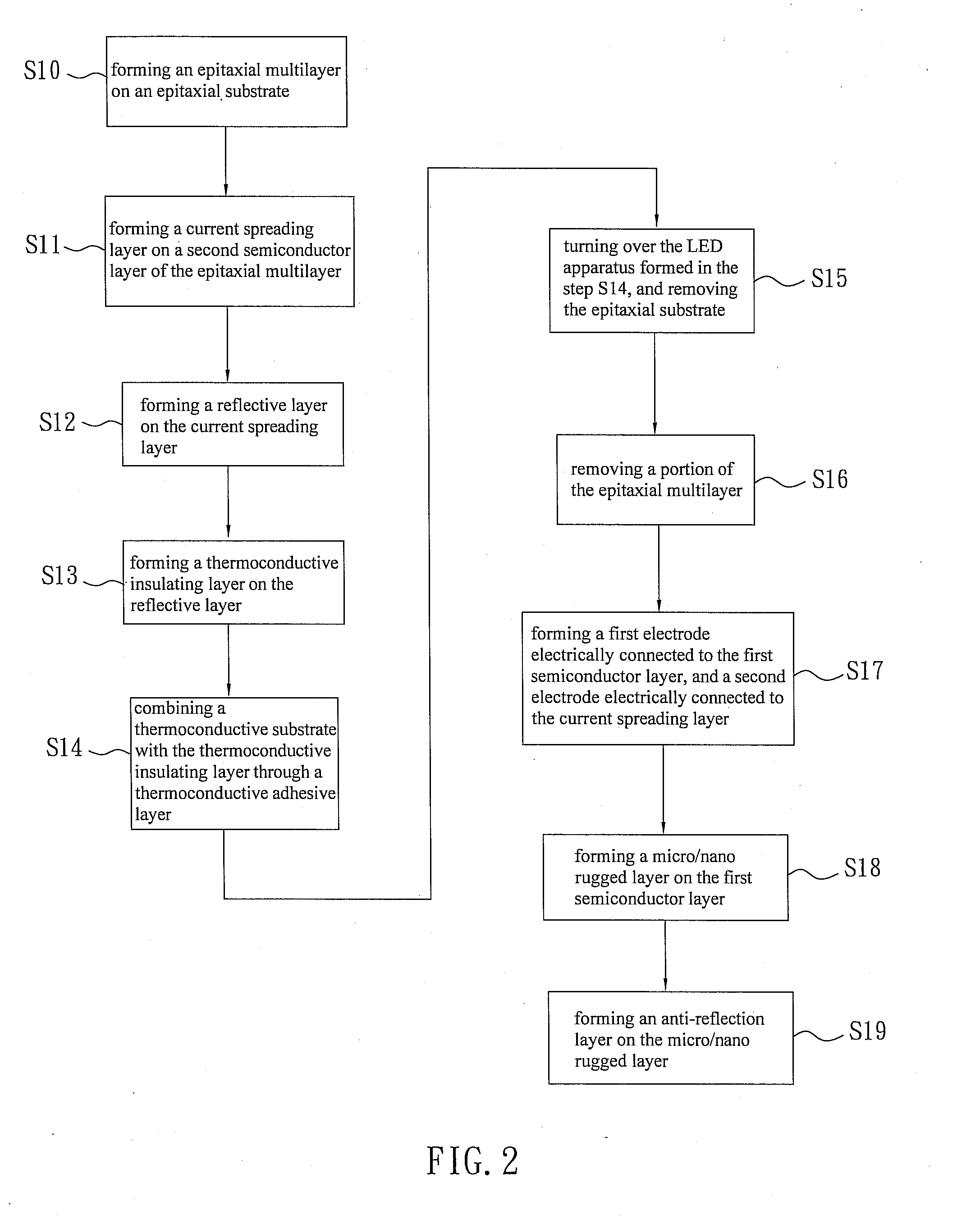
[0022]As shown in FIG. 2, a manufacturing method of a LED apparatus according to a first embodiment of the invention includes steps S10 to S19. Illustrations will be made by referring to FIG. 2 in conjunction with FIGS. 3A to 3K.

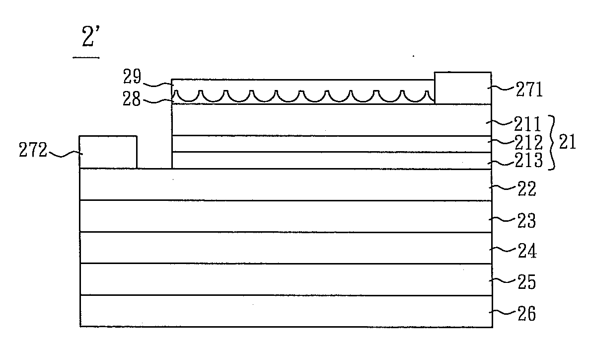
[0023]As shown in FIG. 3A, in step S10, a first semiconductor layer 211 is formed on an epitaxial substrate 20, an active layer 212 is formed on the first semiconductor layer 211, and a second semiconductor layer 213 is formed on the active layer 212. The first semiconductor layer 211, the active layer 212 and the second semiconductor layer 213 constitute an epitaxial multilayer 21. In this embodiment, the first semiconductor layer 211 and the second semiconductor layer 213 can be respectively a P-type epitaxial layer and an N-type epitaxial layer, or respectively the N-type epitaxial layer and the P-type epitaxial layer.

[0024]As shown in FIG. 3B, in step S11, a current spreading layer 22 is formed on the second semiconductor layer 213. In this embodiment, t...

second embodiment

[0034]Referring to FIG. 4, a manufacturing method of a LED apparatus (a vertical type LED apparatus) according to a second embodiment of the invention includes steps S20 to S27. Illustrations will be made by referring to FIG. 4 in conjunction with FIGS. 5A to 5G.

[0035]As shown in FIG. 5A, in the step S20, an epitaxial multilayer 31 is formed on an epitaxial substrate 30. The epitaxial multilayer 31 is composed of a first semiconductor layer 311, an active layer 312 and a second semiconductor layer 313 in sequence. In this embodiment, the first semiconductor layer 311 and the second semiconductor layer 213 can be respectively a P-type epitaxial layer and an N-type epitaxial layer, or respectively the N-type epitaxial layer and the P-type epitaxial layer.

[0036]In FIG. 5B, the structure after the steps S21 to S23 are performed is illustrated. In step S21, a current spreading layer 32 is formed on the second semiconductor layer 313. In this embodiment, the material of the current spread...


PUM


Abstract

A light-emitting diode (LED) apparatus includes an epitaxial multilayer, a micro / nano rugged layer and an anti-reflection layer. The epitaxial multilayer has a first semiconductor layer, an active layer and a second semiconductor layer in sequence. The micro / nano rugged layer is disposed on the first semiconductor layer of the epitaxial multilayer. The anti-reflection layer is disposed on the micro / nano rugged layer. In addition, a manufacturing method of the LED apparatus is also disclosed.

Description

CROSS REFERENCE TO RELATED APPLICATIONS[0001]This Non-provisional application claims priority under 35 U.S.C. §119(a) on Patent Application No(s). 096117765 filed in Taiwan, Republic of China on May 18, 2007, the entire contents of which are hereby incorporated by reference.BACKGROUND OF THE INVENTION[0002]1. Field of Invention[0003]The invention relates to a light-emitting diode (LED) apparatus having a current spreading layer with a micro / nano rugged layer, and a manufacturing method thereof.[0004]2. Related Art[0005]A light-emitting diode (LED) apparatus is a lighting apparatus made of semiconductor materials. The LED apparatus pertains to a cold lighting apparatus, has the advantages of low power consumption, long lifetime, light response speed and small size, and can be manufactured into an extremely small or array-type apparatus. With the continuous progress of the recent technology, the application range thereof covers an indicator of a computer or a house appliance product, ...

Claims


Application Information

Patent Timeline
Patent Type & Authority Applications(United States)
IPC IPC(8): H01L33/00H01L33/22H01L33/44
CPCH01L33/22H01L2933/0091H01L33/44
Inventor CHEN, SHIH-PENGSHIUE, CHING-CHUANCHEN, CHAO-MINWANG, HORNG-JOUCHEN, HUANG-KUN
Owner DELTA ELECTRONICS INC
Why Eureka
Try Eureka