
Display device, chamfering resistance circuit and implementation method thereof

A display device and resistance circuit technology, applied in static indicators, instruments, etc., can solve the problems of increasing the cost of resistance components on the PCB and the cost of packaging, etc.

Active Publication Date: 2019-04-19
HKC CORP LTD
View PDF6 Cites 0 Cited by
  • Summary
  • Abstract
  • Description
  • Claims
  • Application Information

AI Technical Summary

Problems solved by technology

[0004] In view of this, the embodiment of the present application provides a display device and its chamfering resistor circuit and implementation method, aiming to solve the existing problem of obtaining the required resistance value by setting a plurality of parallel chamfering resistors on the PCB to realize the The method of cutting the angle of the gate voltage increases the component cost and the cost of the assembly of the resistor on the PCB, and it is necessary to control the different angle-cutting resistors separately.

Method used


Image

  • Display device, chamfering resistance circuit and implementation method thereof
  • Display device, chamfering resistance circuit and implementation method thereof
  • Display device, chamfering resistance circuit and implementation method thereof

Examples


Embodiment Construction

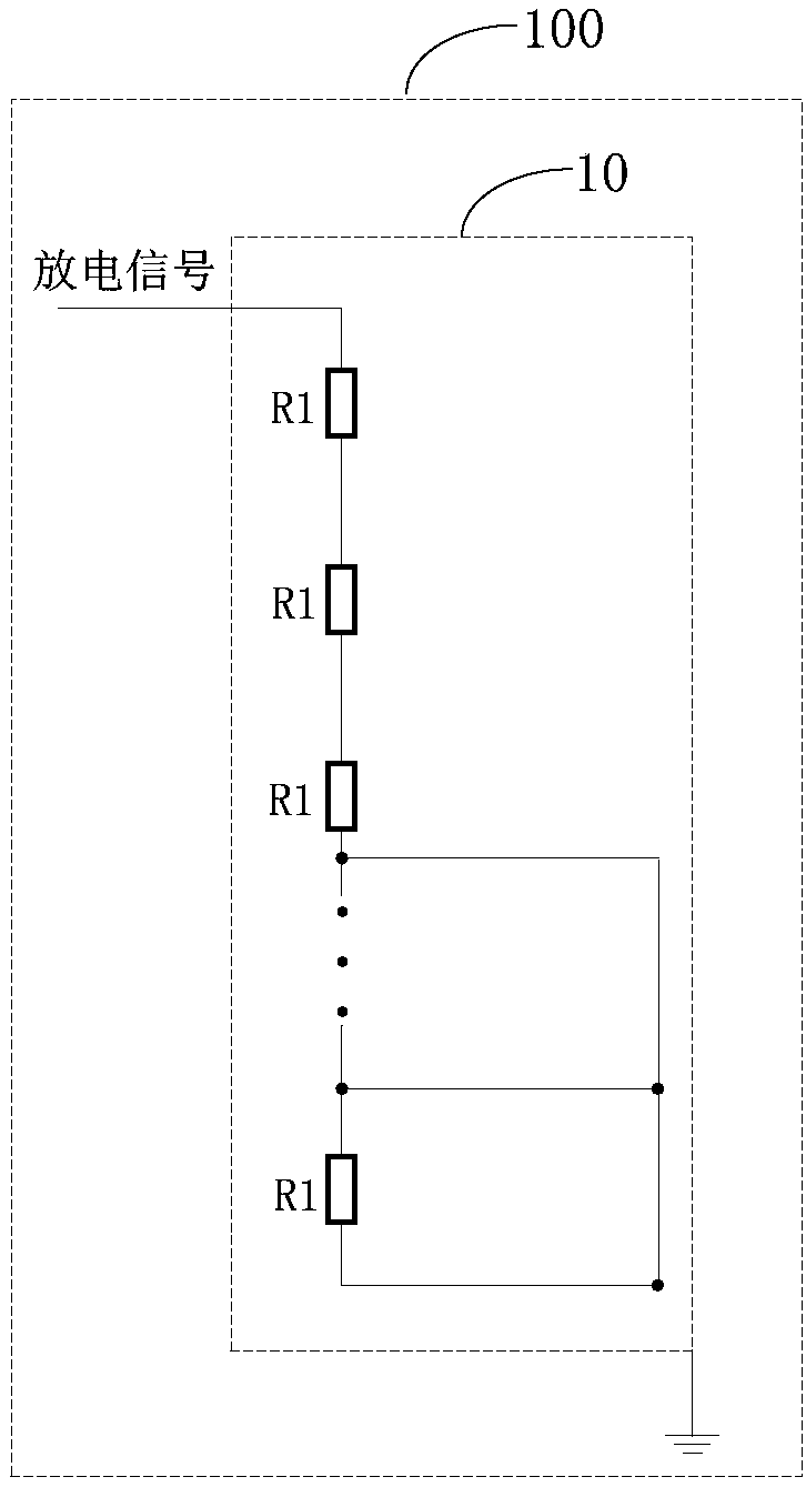
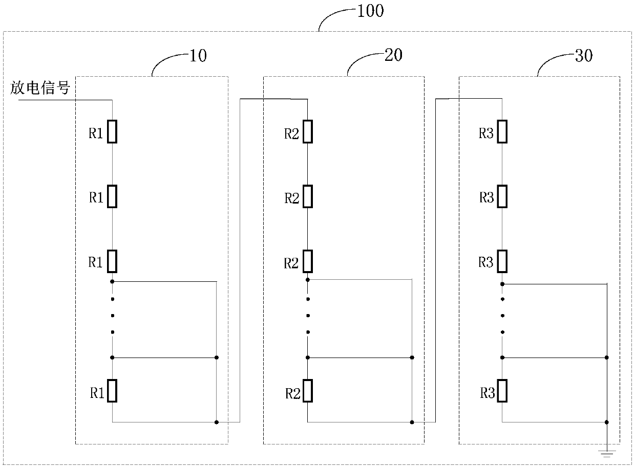
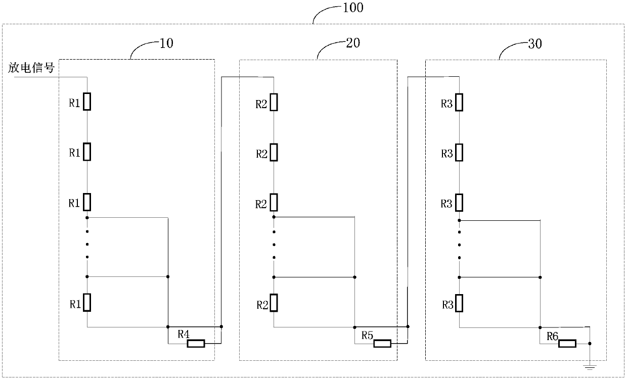
[0054] In order to enable those skilled in the art to better understand the solution of the application, the technical solution in the embodiment of the application will be clearly described below in conjunction with the drawings in the embodiment of the application. Obviously, the described embodiment is the Some examples, but not all examples. Based on the embodiments in this application, all other embodiments obtained by persons of ordinary skill in the art without creative efforts shall fall within the scope of protection of this application.

[0055] The terms "comprising" and any variations thereof in the specification and claims of the present application and the above drawings are intended to cover non-exclusive inclusion. For example, a process, method or system, product or device comprising a series of steps or units is not limited to the listed steps or units, but optionally also includes steps or units not listed, or optionally further includes Other steps or unit...


PUM


Abstract

The present application provides a display device, a chamfering resistance circuit and an implementation method thereof. The chamfering resistance circuit comprises a first area disposed in a fan-outarea of the display device, the first area comprises M1 cascaded first resistors, an input end of a first resistor is an input end of the first area, the input end of the first area is connected to adischarge signal, the output ends of the I1th to the M1th first resistors are jointly connected to form an output end of the first area, and the output end of the first area is grounded, wherein I1 isnot smaller than 1 and not greater than M1, and M1 and I1 are integers. In the present application, according to a resistance value required for chamfering gate voltage, a chamfering resistance circuit composed of a plurality of resistor strings in series and parallel is disposed in the fan-out area of a printed circuit board of the display device to realize a gate voltage chamfering function, sothat batch control of all resistors can be realized, and component cost and packing cost of setting resistors on the printed circuit board can be saved.

Description

technical field [0001] The present application belongs to the field of display technology, and in particular relates to a display device, a chamfering resistance circuit and a realization method thereof. Background technique [0002] With the continuous development of science and technology, various display devices emerge in an endless stream, bringing great convenience to people's production and life. For example, TFT-LCD (thin film transistor-liquid crystal display, thin film transistor-liquid crystal display) is one of the current main types of display devices and is widely used in various display products. TFF-LCD mainly transmits the three primary color compression signals, control signals and power signals to the TCON (Timing Controller, Timing Controller) chip set on the PCB (Printed Circuit Board) through its system main board. The S-COF (Source-Chip on Film, source driver chip) and G-COF (Gate-Chip onFilm, gate driver chip) set on the PCB are processed and output t...

Claims


Application Information

Patent Timeline
Patent Type & Authority Applications(China)
IPC IPC(8): G09G3/20G09G3/36
CPCG09G3/20G09G3/3677G09G2310/0264
Inventor 黄笑宇
Owner HKC CORP LTD
Learn More