A kind of LED lamp sealing glue printing process

A LED lamp and glue sealing technology, which is applied in the direction of adhesives, film/sheet adhesives, non-polymer adhesive additives, etc., can solve the problem of inaccurate alignment of the injection port, poor cavity filling, and unfavorable Problems such as industrial production, to achieve the effect of improving surface roughness, increasing strength, and better anti-adhesive effect

Active Publication Date: 2020-02-21
东莞市谷麦光学科技有限公司 +3
View PDF5 Cites 0 Cited by
  • Summary
  • Abstract
  • Description
  • Claims
  • Application Information

AI Technical Summary

Problems solved by technology

For this reason, there is a cavity in the LED base where the LED chip is accommodated. This cavity is the filling place of fluorescent glue. Generally, glue is injected into each cavity by dispensing, but this method is not suitable for the size Smaller LEDs, etc., are prone to glue overflow, or poor alignment of the injection port, resulting in poor filling of some cavities, which is not conducive to the industrial production of LEDs.

Method used


Image

  • A kind of LED lamp sealing glue printing process
  • A kind of LED lamp sealing glue printing process
  • A kind of LED lamp sealing glue printing process

Examples


Embodiment 1

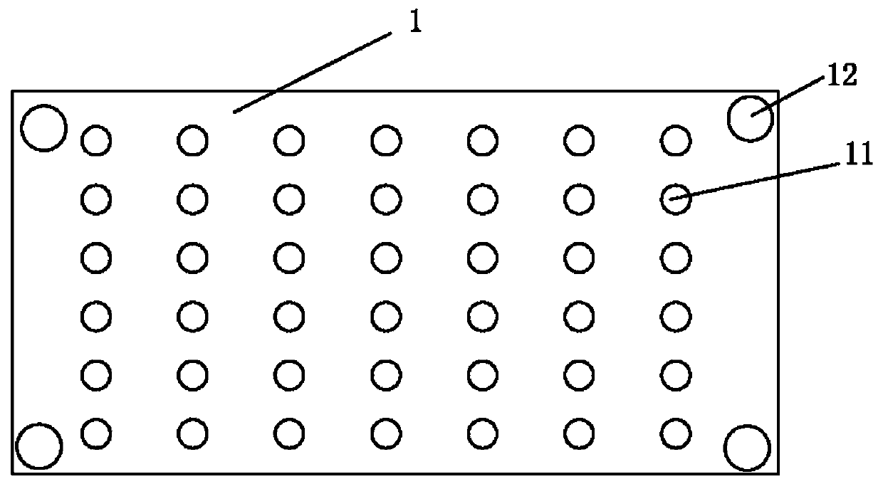
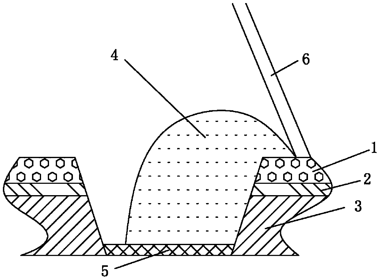
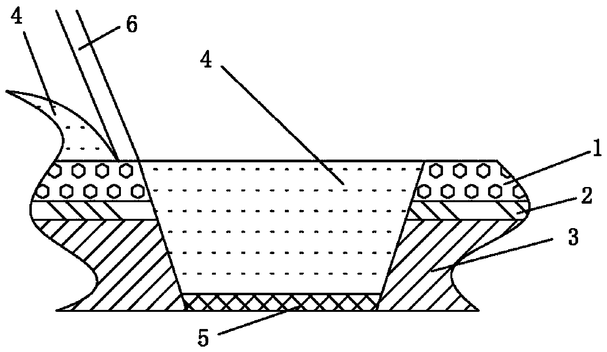
[0051] A LED lamp sealant printing process, the LED lamp includes an LED base 3, the LED base 3 is provided with several cavities, and an LED chip 5 is fixed in each cavity, the printing process includes the following steps:

[0052] (1) design a tape film 1, described tape film 1 is provided with some through holes 11, one deck adhesive layer 2 is coated on one side of described adhesive tape film 1, described adhesive layer 2 and base 3 are carried out Fit and make the through hole 11 face the cavity of the LED base 3;

[0053] (2) Inject fluorescent glue 4 into the cavity;

[0054] (3) scrape coating on the surface of adhesive tape film 1 with scraper 6;

[0055] (4) The tape film 1 is peeled off.

[0056] Wherein, the end of the tape film 1 is also provided with a positioning hole 12 .

[0057] Wherein, described adhesive tape film 1 is made up of the raw material of following parts by weight:

[0058]

[0059] The concrete steps of the preparation method of tape fi...

Embodiment 2

[0083] A LED lamp sealant printing process, the LED lamp includes an LED base 3, the LED base 3 is provided with several cavities, and an LED chip 5 is fixed in each cavity, the printing process includes the following steps:

[0084] (1) design a tape film 1, described tape film 1 is provided with some through holes 11, one deck adhesive layer 2 is coated on one side of described adhesive tape film 1, described adhesive layer 2 and base 3 are carried out Fit and make the through hole 11 face the cavity of the LED base 3;

[0085] (2) Inject fluorescent glue 4 into the cavity;

[0086] (3) scrape coating on the surface of adhesive tape film 1 with scraper 6;

[0087] (4) The tape film 1 is peeled off.

[0088] Wherein, the end of the tape film 1 is also provided with a positioning hole 12 .

[0089] Wherein, described adhesive tape film 1 is made up of the raw material of following parts by weight:

[0090]

[0091] The concrete steps of the preparation method of tape fi...

Embodiment 3

[0115] A LED lamp sealant printing process, the LED lamp includes an LED base 3, the LED base 3 is provided with several cavities, and an LED chip 5 is fixed in each cavity, the printing process includes the following steps:

[0116](1) design a tape film 1, described tape film 1 is provided with some through holes 11, one deck adhesive layer 2 is coated on one side of described adhesive tape film 1, described adhesive layer 2 and base 3 are carried out Fit and make the through hole 11 face the cavity of the LED base 3;

[0117] (2) Inject fluorescent glue 4 into the cavity;

[0118] (3) scrape coating on the surface of adhesive tape film 1 with scraper 6;

[0119] (4) The tape film 1 is peeled off.

[0120] Wherein, the end of the tape film 1 is also provided with a positioning hole 12 .

[0121] Wherein, described adhesive tape film 1 is made up of the raw material of following parts by weight:

[0122]

[0123] The concrete steps of the preparation method of tape fil...


PUM

PropertyMeasurementUnit
particle diameteraaaaaaaaaa
thicknessaaaaaaaaaa

Abstract

The invention relates to the technical field of LEDs, in particular to an LED lamp molding printing process. The LED lamp comprises an LED base, the LED base is provided with a plurality of cavities,and each cavity is fixed with an LED chip. The printing process comprises the following steps of: (1) designing a tape film, wherein the tape film is provided with a plurality of through holes, one surface of the tape film is coated with an adhesive layer, the adhesive is applied to the base to allow the through holes to face the cavities of the LED base; (2) injecting fluorescent glue into the cavities; (3) performing blade coating at the surface of the tape film by employing a scraper; and (4) stripping off the tape film. The tape film is attached to the LED base to prevent the fluorescent glue from pasting to the base; the scraper is employed to scrape the overflowing fluorescent glue on the tape film into the cavities of the LED base to facilitate even glue amount of the cavities so asto display an even luminance effect.

Description

technical field [0001] The invention relates to the technical field of LEDs, in particular to an LED lamp sealant printing process. Background technique [0002] At present, the main method of making white LED lamps is to coat yellow phosphor powder on the surface of blue LED chips, which is excited by blue light to emit yellow light, and then mixed with the transmitted blue light to present white light. For this reason, there is a cavity in the LED base where the LED chip is accommodated. This cavity is the filling place of fluorescent glue. Generally, glue is injected into each cavity by dispensing, but this method is not suitable for the size Smaller LEDs, etc., are prone to adverse situations such as overflow of glue, or inaccurate alignment of the glue injection port, resulting in poor filling of some cavities, which is not conducive to the industrial production of LEDs. Contents of the invention [0003] In order to overcome the shortcomings and deficiencies in the ...

Claims


Application Information

Patent Timeline
Patent Type & Authority Patents(China)
IPC IPC(8): H01L33/50H01L33/52C09J7/30C09J7/25C09J4/02C09J4/06C09J11/04C08L67/02C08L33/12C08K13/06C08K9/06C08K3/34C08K3/36
CPCC08K2201/011C08L67/02C09J4/06C09J7/255C09J7/30C09J11/04C09J2467/00H01L33/50H01L33/52H01L2933/0041H01L2933/005C08L33/12C08K13/06C08K9/06C08K3/346C08K3/36
Inventor 李萌萌张坤廖勇军张喜光
Owner 东莞市谷麦光学科技有限公司
Why Eureka
Try Eureka