Display panel
A display panel and substrate technology, applied in nonlinear optics, instruments, optics, etc., can solve the problems of easy deformation of the planarization layer, poor pressure resistance of the display panel, etc., and achieve the effect of improving the pressure resistance
- Summary
- Abstract
- Description
- Claims
- Application Information
AI Technical Summary
Problems solved by technology
Method used
Image

Examples
Embodiment Construction
[0027] The technical solutions in the embodiments of the present application will be clearly and completely described below in conjunction with the drawings in the embodiments of the present application. Apparently, the described embodiments are only some of the embodiments of this application, not all of them. Based on the embodiments in this application, all other embodiments obtained by those skilled in the art without making creative efforts belong to the scope of protection of this application.
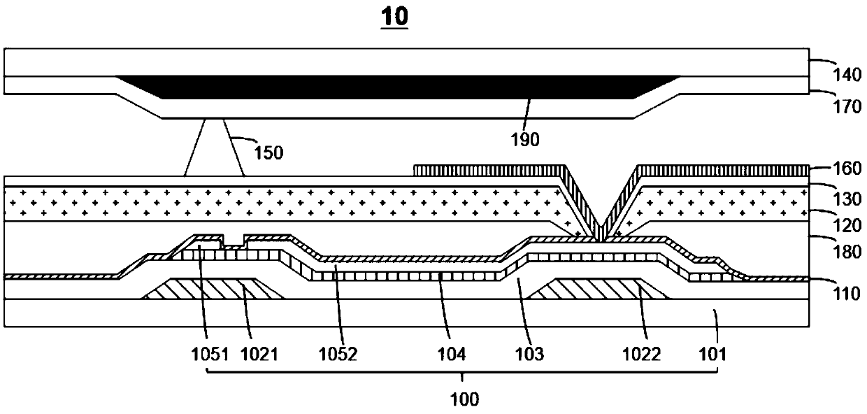
[0028] see figure 1 , which is a schematic structural diagram of the display panel 10 according to the first embodiment of the present application, and the display panel 10 includes:
[0029] Array substrate 100;
[0030] a passivation layer 110, the passivation layer 110 is disposed on the array substrate 100;
[0031] a planarization layer 120, the planarization layer 120 is disposed on the passivation layer 110;
[0032] A pressure-resistant layer 130, the pressure-resista...
PUM
| Property | Measurement | Unit |
|---|---|---|
| thickness | aaaaa | aaaaa |
| thickness | aaaaa | aaaaa |
Abstract
Description
Claims
Application Information
 - R&D Engineer
- R&D Manager
- IP Professional
- Industry Leading Data Capabilities
- Powerful AI technology
- Patent DNA Extraction
Browse by: Latest US Patents, China's latest patents, Technical Efficacy Thesaurus, Application Domain, Technology Topic.
© 2024 PatSnap. All rights reserved.Legal|Privacy policy|Modern Slavery Act Transparency Statement|Sitemap