A design method and system for improving crosstalk measurement between signal lines on a PCB
A technology of PCB board and design method, which is applied in the design method and system field of improving crosstalk measurement between signal lines on PCB board, and can solve the problems of insufficient accuracy of measurement results, low efficiency of crosstalk measurement between signal lines, etc.
- Summary
- Abstract
- Description
- Claims
- Application Information
AI Technical Summary
Problems solved by technology
Method used
Image

Examples
Embodiment Construction
[0033] In order to enable those skilled in the art to better understand the technical solutions in the application, the following will clearly and completely describe the technical solutions in the embodiments of the application with reference to the drawings in the embodiments of the application. Obviously, the described The embodiments are only a part of the embodiments of the present application, rather than all the embodiments. Based on the embodiments in this application, all other embodiments obtained by those of ordinary skill in the art without creative work should fall within the protection scope of this application.
[0034] In order to better understand the present application, the embodiments of the present application are explained in detail below in conjunction with the drawings.
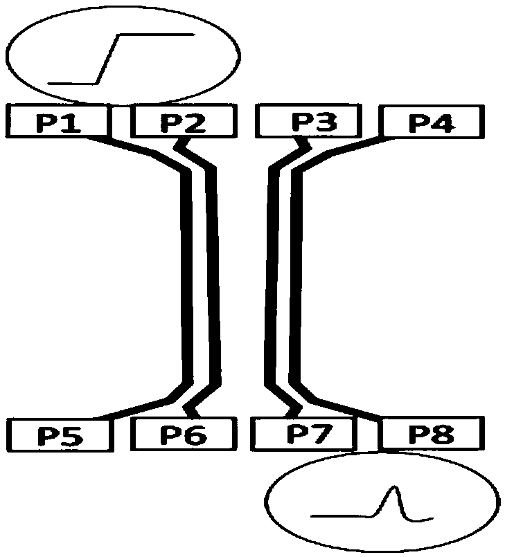
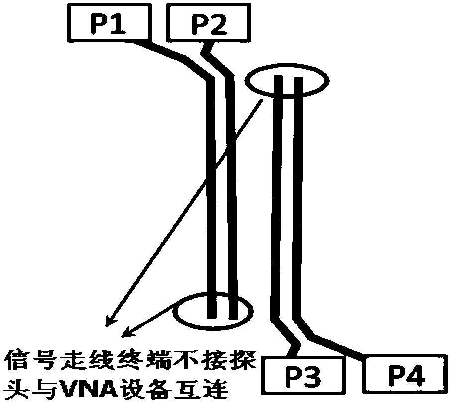
[0035] See Figure 5 , Figure 5 This is a schematic flow chart of a design method for improving the measurement of crosstalk between signal lines on a PCB provided by an embodiment of this...
PUM
 Abstract
Description
Claims
Application Information
 - R&D Engineer
- R&D Manager
- IP Professional
- Industry Leading Data Capabilities
- Powerful AI technology
- Patent DNA Extraction
Browse by: Latest US Patents, China's latest patents, Technical Efficacy Thesaurus, Application Domain, Technology Topic.
© 2024 PatSnap. All rights reserved.Legal|Privacy policy|Modern Slavery Act Transparency Statement|Sitemap