PCB positioning error calibration method, device and equipment and storage medium

A PCB board and positioning error technology, applied in the field of devices, equipment and storage media, and PCB board positioning error calibration method, can solve the problems of image printing offset error, etc., and achieve the effect of small error, simple operation and high efficiency

Pending Publication Date: 2019-04-26
SENDA SHENZHEN TECH CO LTD
View PDF9 Cites 15 Cited by
  • Summary
  • Abstract
  • Description
  • Claims
  • Application Information

AI Technical Summary

Problems solved by technology

[0003] The embodiment of the present invention provides a PCB board positioning error calibration method, device, equipment, and storage medium to solve the problem of offset errors in image printing caused by inaccurate PCB board positioning in the prior art

Method used


Image

  • PCB positioning error calibration method, device and equipment and storage medium
  • PCB positioning error calibration method, device and equipment and storage medium
  • PCB positioning error calibration method, device and equipment and storage medium

Examples


Embodiment Construction

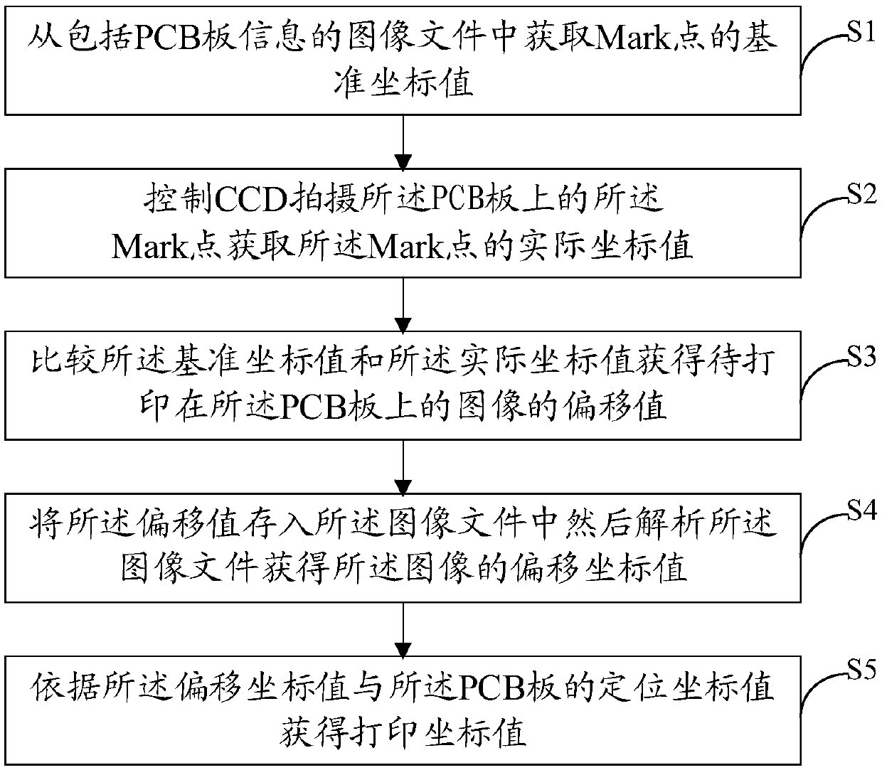
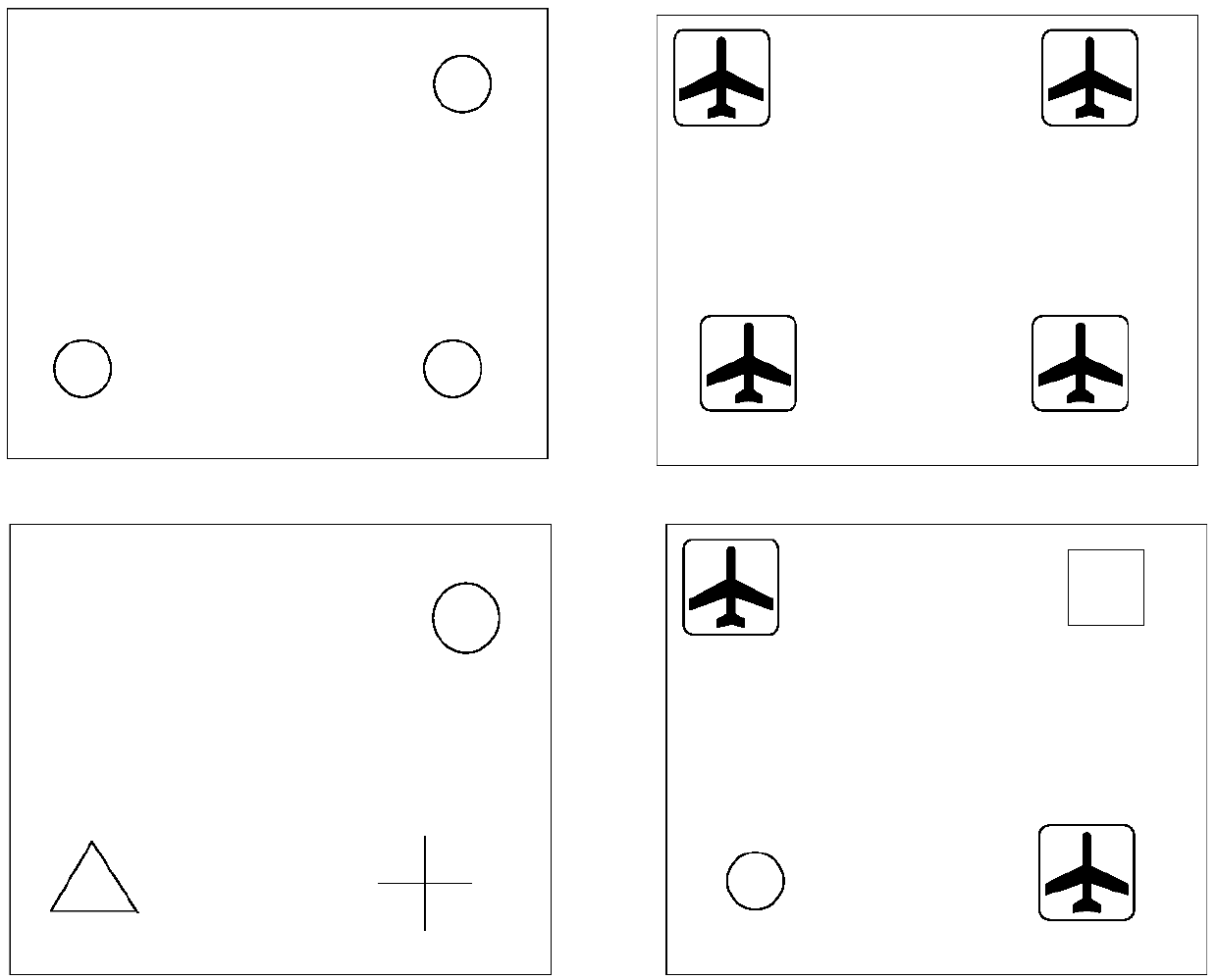
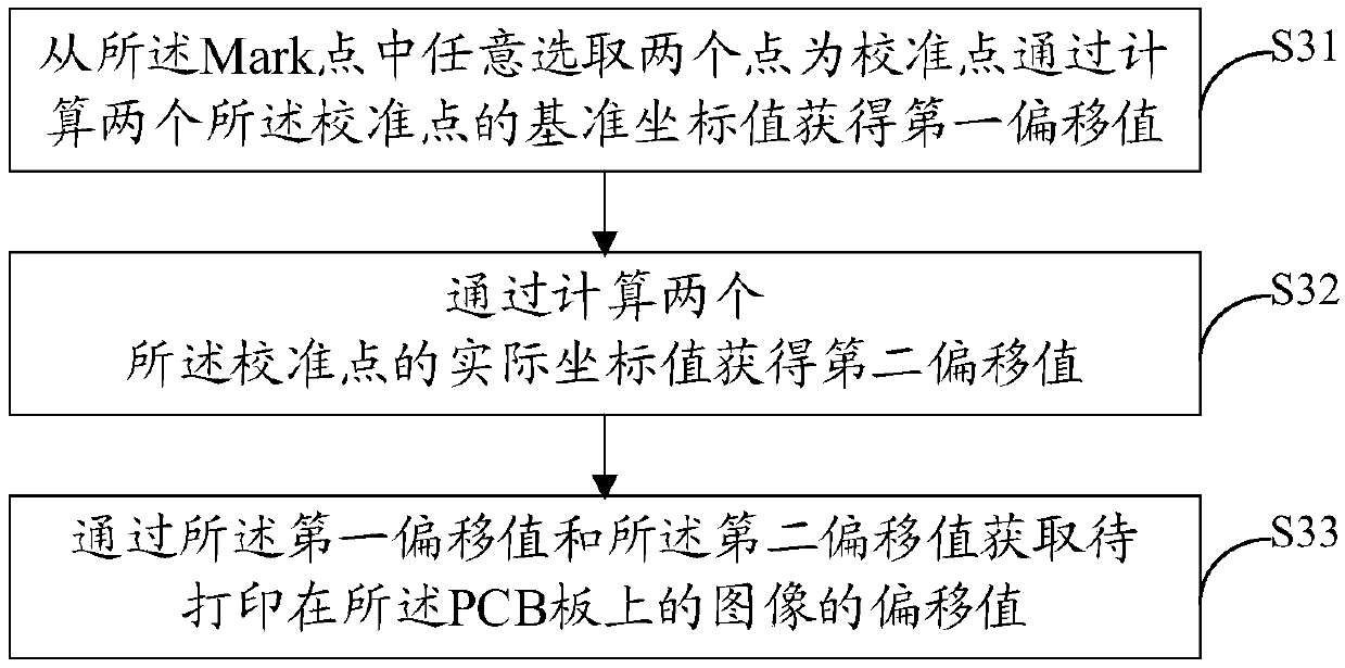
[0049] The characteristics and exemplary embodiments of various aspects of the present invention will be described in detail below. In order to make the purpose, technical solutions and advantages of the present invention more clear, the present invention will be further described in detail below in conjunction with the accompanying drawings and embodiments. It should be understood that the specific embodiments described here are only configured to explain the present invention, not to limit the present invention. It will be apparent to one skilled in the art that the present invention may be practiced without some of these specific details. The following description of the embodiments is only to provide a better understanding of the present invention by showing examples of the present invention.

[0050]It should be noted that, in this document, relational terms such as first and second are only used to distinguish one entity or operation from another entity or operation, and...


PUM


Abstract

The invention discloses a PCB positioning error calibration method, device and equipment and a storage medium. The method comprises the steps of obtaining a reference coordinate value of a Mark pointfrom an image file comprising PCB information; Controlling a CCD to shoot the Mark point on the PCB to obtain an actual coordinate value of the Mark point; Comparing the reference coordinate value with the actual coordinate value to obtain an offset value of an image to be printed on the PCB; Storing the offset value in the image file, and analyzing the image file to obtain an offset coordinate value of the image; And obtaining a printing coordinate value according to the offset coordinate value and the positioning coordinate value of the PCB. According to the method, manual participation is not needed, automation is high, efficiency is high, and the printing position of the image on the PCB is accurate after recalculation.

Description

technical field [0001] The invention relates to the technical field of inkjet printing, in particular to a PCB board positioning error calibration method, device, equipment and storage medium. Background technique [0002] When printing the characters on the PCB board, since the position of the PCB board is easily shifted manually, the characters cannot be printed in the exact position when printing the characters. In order to print characters accurately, certain measures must be taken to accurately position the PCB board. In the PCB board design stage, designers usually make Mark points as positioning references. Only with accurate positional relationships can they be used for subsequent effective detection. Do the basics. For the problem of offset in manual PCB board placement, the existing method is to determine the moving distance of the motor through the Mark point on the PCB board, and then move the PCB board through the motor to place the board in an accurate positio...

Claims


Application Information

Patent Timeline
Patent Type & Authority Applications(China)
IPC IPC(8): G06T7/00G06T7/70
CPCG06T7/0004G06T2207/10004G06T2207/30141G06T7/70
Inventor 左国云陈艳黄振金
Owner SENDA SHENZHEN TECH CO LTD
Why Eureka
Try Eureka