Three-dimensional memory device and preparation method thereof

A three-dimensional storage and device technology, applied in the direction of electric solid-state devices, semiconductor devices, electrical components, etc., can solve the problem that the bottom of the channel hole cannot be opened and electrically connected to the substrate, and the side wall of the channel hole and its filling can be easily damaged. , channel holes are not easy to accurately align, etc., to achieve the effect of shortening the process cycle, high yield rate, and good structure

Active Publication Date: 2019-05-03
YANGTZE MEMORY TECH CO LTD
View PDF3 Cites 37 Cited by
  • Summary
  • Abstract
  • Description
  • Claims
  • Application Information

AI Technical Summary

Problems solved by technology

However, usually the upper and lower stacked channel holes are not easy to be precisely aligned, and when the alignment is not good, it is easy to damage the side walls of the channel holes and their fillings (especially at their dislocations); more seriously, When the channel holes of the upper and lower stacks are extremely poorly aligned, it is almost impossible to perform the etching process to open the bottom of the channel hole and electrically connect to the substrate, which will cause the memory cell to fail

Method used


Image

  • Three-dimensional memory device and preparation method thereof
  • Three-dimensional memory device and preparation method thereof
  • Three-dimensional memory device and preparation method thereof

Examples


Embodiment Construction

[0037] Specific embodiments of the present invention will be described in more detail below with reference to the accompanying drawings. Although exemplary embodiments of the invention are shown in the drawings, it should be understood that the invention may be practiced in other ways than those described herein, and therefore, the invention is not limited by the following embodiments.

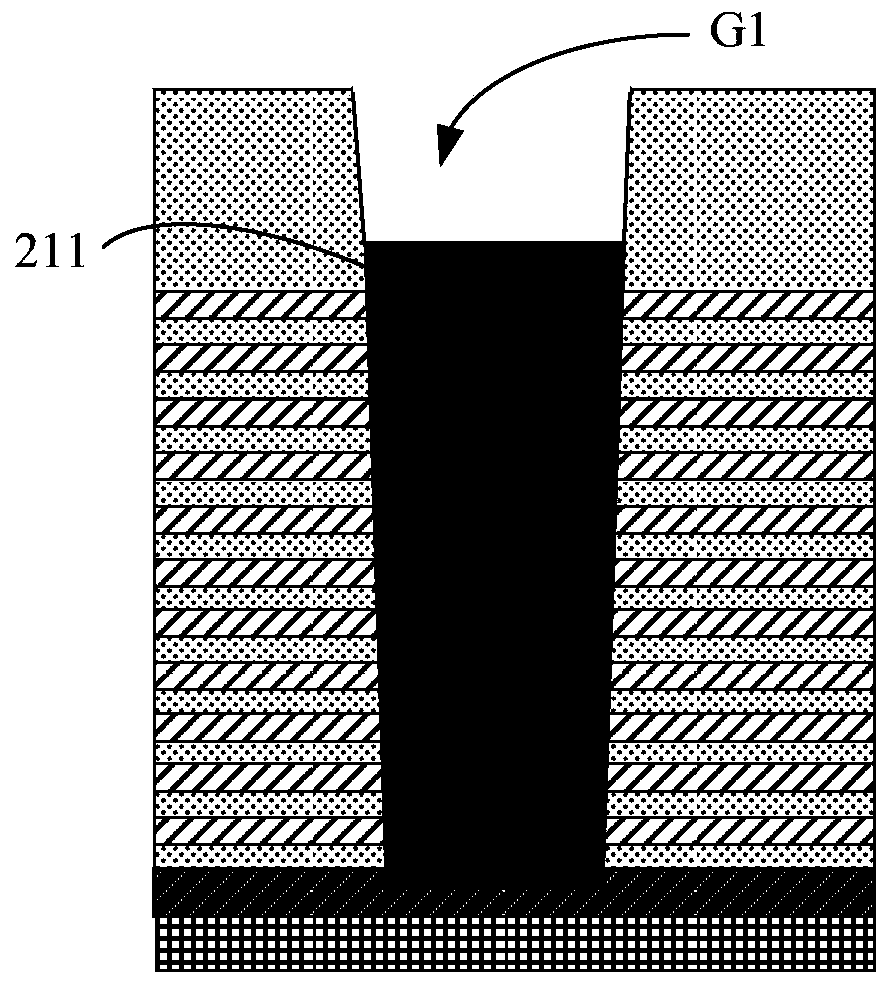
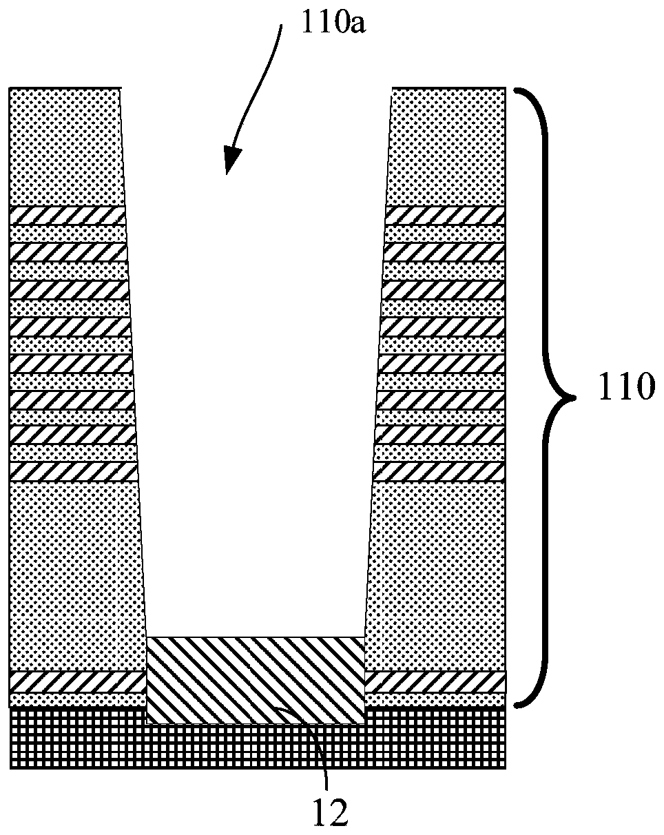
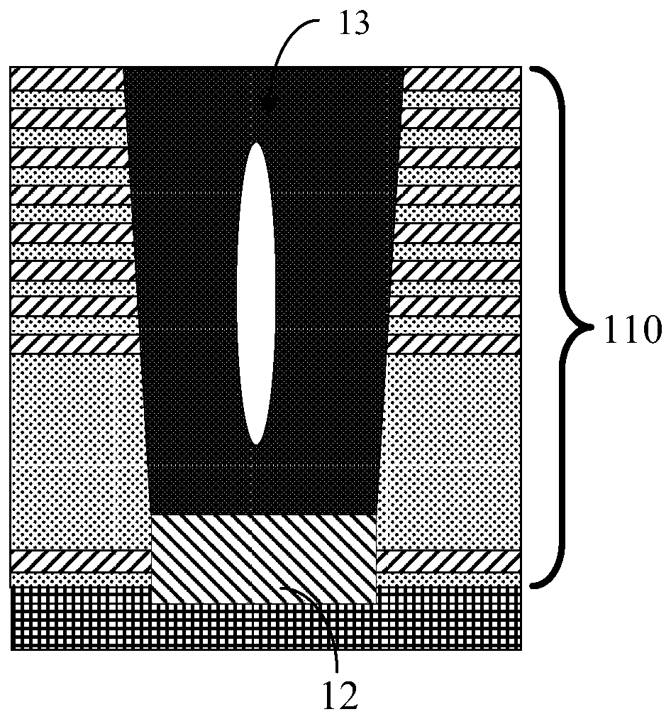
[0038] Before describing the specific implementation of the present invention, first briefly introduce the single-channel preparation process commonly used in the industry in three-dimensional memory devices: grow an epitaxial structure 12 at the bottom of the lower layer channel hole 110a of the lower layer stack 110 (see Figure 1a ), and fill the sacrificial material 13 on the epitaxial structure 12 (see Figure 1b ); then form an upper layer stack 120 and an upper layer channel hole 120a corresponding to the lower layer channel hole 110a on the lower layer stack 110 (see Figure 1c ), and...


PUM


Abstract

The invention provides a preparation method of a three-dimensional memory device. The method includes the following steps: sequentially forming an etching stop layer, a first stack, and first channelholes exposing the etching stop layer on a first substrate; forming a first polysilicon plug on a first sacrificial material layer filled in each of the first channel holes, and disposing a carrier wafer thereon; removing the first substrate, and forming a second stack and second channel holes on the other side of the etching stop layer to expose the etching stop layer; removing the etching stop layer between each of the first channel holes and each of the second channel holes, and removing the first sacrificial material layer; covering sidewalls of the first channel holes and the second channel holes with protective layers, and etching parts of the first stack and the second stack exceeding the remaining etching stop layer along radial directions of the channel holes, and removing the protective layers to form a through channel hole; and filling the through channel hole form a single channel. The invention also provides the three-dimensional memory device.

Description

technical field [0001] The invention relates to the technical field of semiconductor devices, in particular to a three-dimensional storage device and a preparation method thereof. Background technique [0002] A three-dimensional (3D) structured memory has a high integration density and a large storage capacity because memory cells are three-dimensionally arranged on a substrate, and thus has been more widely used in electronic products. In the single channel formation (single channel formation) of the three-dimensional flash memory device, the etching of the channel hole is carried out between the stack (deck) and the stack, during this period, the channel hole of the lower stack is temporarily filled with a sacrificial material, After the upper and lower stacks are etched open, the sacrificial material is removed, and the formed channel holes are filled together. However, usually the upper and lower stacked channel holes are not easy to be precisely aligned, and when the ...

Claims


Application Information

Patent Timeline
Patent Type & Authority Applications(China)
IPC IPC(8): H01L27/115H01L27/11582H01L27/11568
Inventor 肖莉红刘沙沙
Owner YANGTZE MEMORY TECH CO LTD
Why Eureka
Try Eureka