

Integrated packaged semiconductor device
- Summary
- Abstract
- Description
- Claims
- Application Information
AI Technical Summary
Problems solved by technology
Method used
Image

Examples
Embodiment Construction
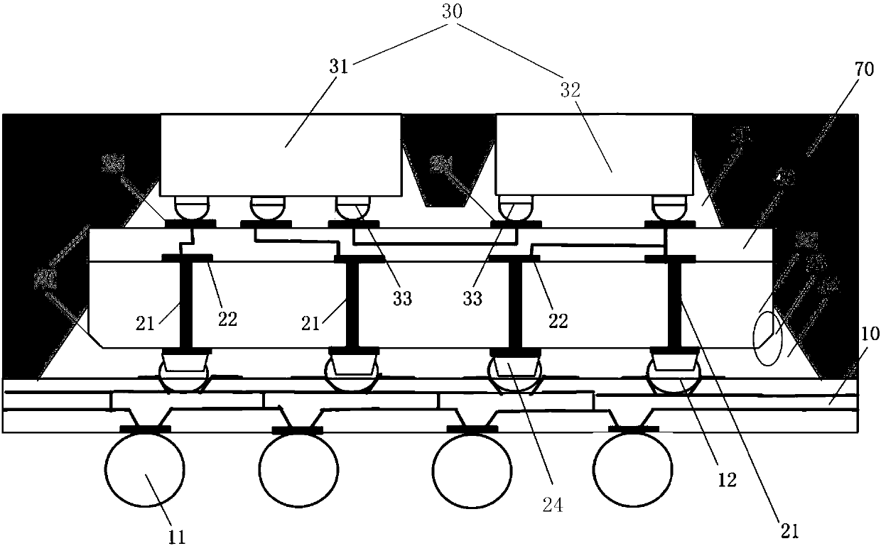
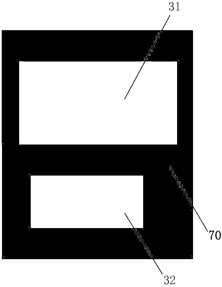
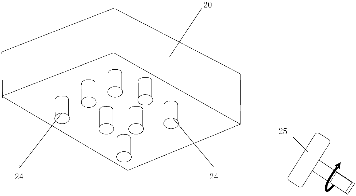
[0045] In the following, only some exemplary embodiments are briefly described. As those skilled in the art would realize, the described embodiments may be modified in various different ways, all without departing from the spirit or scope of the present invention. Accordingly, the drawings and descriptions are to be regarded as illustrative in nature and not restrictive.
[0046] In describing the present invention, it should be understood that the terms "center", "longitudinal", "transverse", "length", "width", "thickness", "upper", "lower", "front", " Back", "Left", "Right", "Vertical", "Horizontal", "Top", "Bottom", "Inner", "Outer", "Clockwise", "Counterclockwise", "Axial" , "radial", "circumferential" and other indicated orientations or positional relationships are based on the orientations or positional relationships shown in the drawings, which are only for the convenience of describing the present invention and simplifying the description, rather than indicating or im...
PUM
 Abstract
Description
Claims
Application Information