

Display device and preparation method thereof
A display device and packaging layer technology, which is applied in the manufacture of semiconductor/solid-state devices, electrical components, and electric solid-state devices, etc., can solve the problems of easy entry of water and oxygen into the interior of the device, poor sealing effect of the display device, affecting the performance and life of the device, etc. To achieve the effect of easy operation, improve the use effect, and ensure the use effect
- Summary
- Abstract
- Description
- Claims
- Application Information
AI Technical Summary
Problems solved by technology
Method used
Image

Examples
Embodiment 1
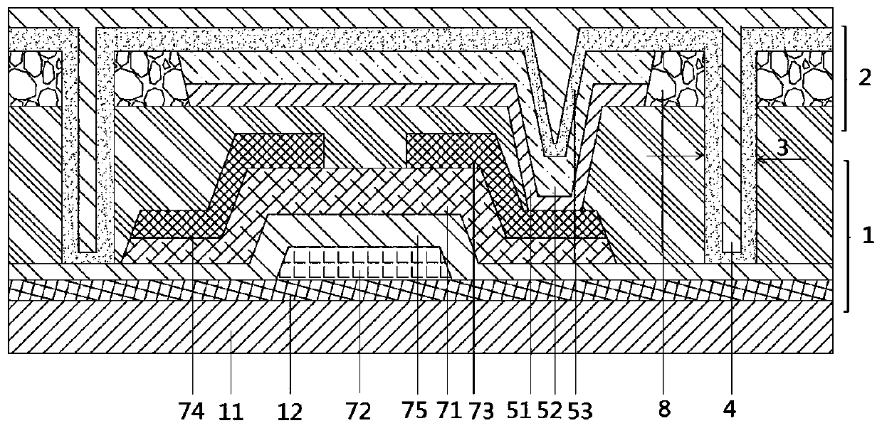
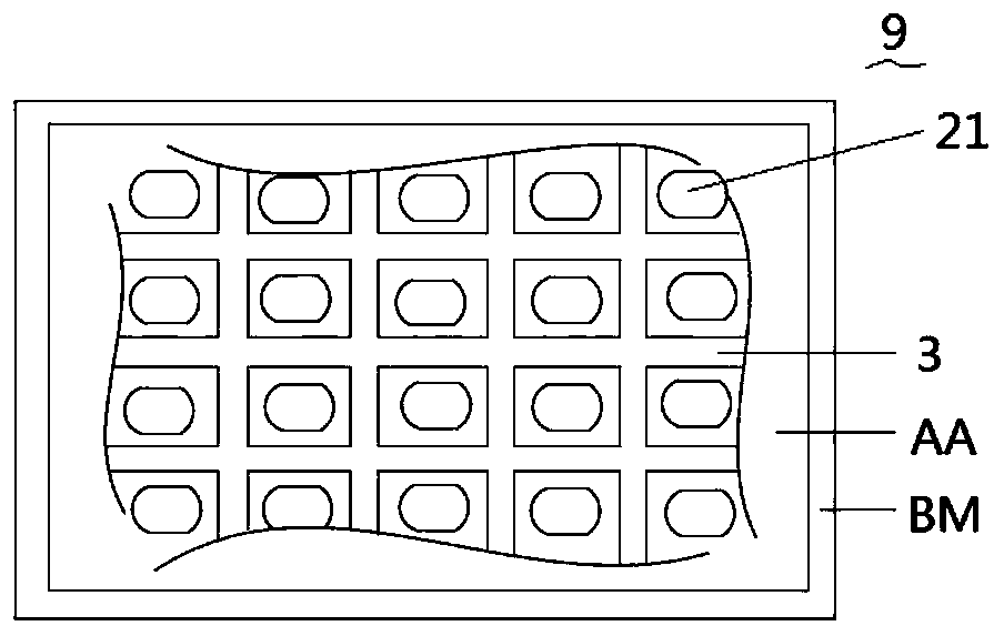
[0045] This embodiment provides a display device, such as figure 1 and figure 2 As shown, it includes a plurality of organic light emitting diodes 21 and an encapsulation layer 4 for encapsulating the organic light emitting diodes on the substrate 11 . The display device also includes at least one encapsulation unit, each encapsulation unit encapsulates an organic light emitting diode 21, and the side wall of the encapsulation unit is surrounded by a groove 3 along a direction perpendicular to the light-emitting surface of the corresponding organic light emitting diode 21, and the organic light emitting diode 21 The second electrode layer 53 in the corresponding organic light emitting diode 21 extends into the groove 3 along the top.
[0046] The organic light-emitting diodes 21 arranged in the same layer form the display array layer 2, and correspondingly, it also includes a driving array layer 1 stacked on the substrate 11; the driving array layer 1 includes a number of ju...
Embodiment 2
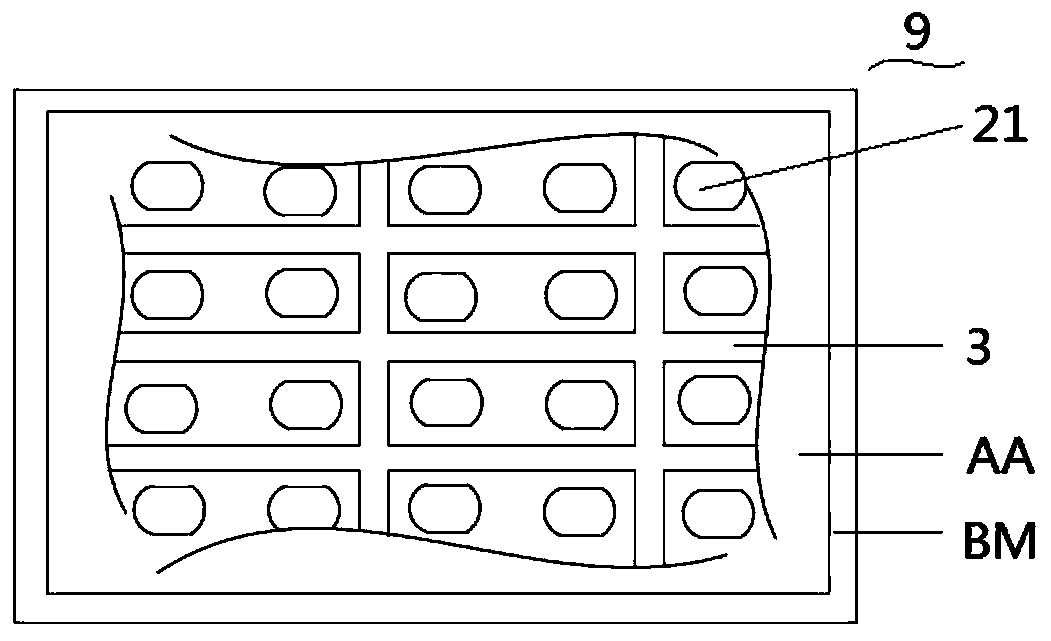
[0088] This embodiment provides a display device, such as image 3 As shown, its structure is basically the same as that of the display device provided in Embodiment 1. The difference is that each encapsulation unit encapsulates two laterally adjacent organic light emitting diodes 21, thus forming an encapsulation barrier with an encapsulation layer 4 vertically, even the most The encapsulation of the peripheral organic light-emitting diodes fails, and water vapor / oxygen will not continue to penetrate into the display area, and the light emission of the internal organic light-emitting diodes will not be affected, and the encapsulation effect will be better.
[0089] The preparation method of the display device is the same as in Example 1, the difference is that the mask in the photolithography step needs to be replaced in step S3, and the mask opening in this step in Example 1 corresponds to an organic light emitting diode, and step S3 in this example The mask openings in corr...
Embodiment 3
[0093] This embodiment provides a display device, such as Figure 4 As shown, its structure is basically the same as that of the display device provided in Embodiment 1. The difference is that each encapsulation unit encapsulates four adjacent organic light-emitting diodes 21, thus forming an encapsulation barrier with an encapsulation layer 4 vertically, even if the outermost The organic light-emitting diode packaging fails, and the water vapor / oxygen will not continue to penetrate into the display area, the internal organic light-emitting diodes will not be affected by the light emission, and the packaging effect will be better.
[0094] The preparation method of the display device is the same as in Example 1, the difference is that the mask in the photolithography step needs to be replaced in step S3, and the mask opening in this step in Example 1 corresponds to an organic light emitting diode, and step S3 in this example The mask openings in correspond to the openings of t...
PUM
| Property | Measurement | Unit |
|---|---|---|
| Thickness | aaaaa | aaaaa |
| Thickness | aaaaa | aaaaa |
| Thickness | aaaaa | aaaaa |
Abstract
Description
Claims
Application Information