Display panel and touch display device
A display panel and display area technology, which is applied in optics, instruments, electrical digital data processing, etc., can solve the problems of inconspicuous improvement and achieve the effect of reducing the impact
- Summary
- Abstract
- Description
- Claims
- Application Information
AI Technical Summary
Problems solved by technology
Method used
Image
Examples
Embodiment 1
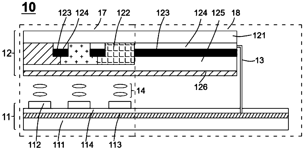
[0039] see figure 1 , which is the display panel 10 according to the first embodiment of the present application. The display panel 10 includes an array substrate 11 and a color filter substrate 12 arranged oppositely. The color filter substrate 12 includes:
[0040] The first substrate 121, the first substrate 121 has a display area 17 and a non-display area 18 located on the periphery of the display area 17;
[0041] A color film layer 122, the color film layer 122 includes a plurality of color filter units, the color film layer 122 is formed on the display area 17 of the first substrate 121;
[0042] A black matrix layer 123, the black matrix layer 123 is formed between adjacent color filter units and the non-display area 18 of the first substrate 121;
[0043] A conductive layer 124, the conductive layer 124 is arranged between the first substrate 121 and the black matrix layer 123 and the black matrix layer 123 covers the conductive layer 124;
[0044] The array substra...
Embodiment 2
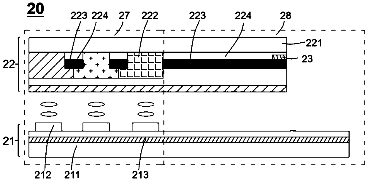
[0057] see image 3 , which is the display panel 20 of the second embodiment of the present application. The display panel 20 includes an array substrate 21 and a color filter substrate 22 arranged oppositely. The color filter substrate 22 includes:
[0058] The first substrate 221, the first substrate 221 has a display area 27 and a non-display area 28 located on the periphery of the display area 27;
[0059] A color film layer 222, the color film layer 222 includes a plurality of color filter units, the color film layer 222 is formed on the display area 27 of the first substrate 221;
[0060] A black matrix layer 223, the black matrix layer 223 is formed between adjacent color filter units and the non-display area 28 of the first substrate 221;
[0061] A conductive layer 224, the conductive layer 224 is arranged between the first substrate 221 and the black matrix layer 223 and the black matrix layer 223 covers the conductive layer 224;
[0062] The array substrate 21 inc...
Embodiment 3
[0065] see Figure 4 , which is the display panel 30 of the third embodiment of the present application. The display panel 30 includes an array substrate 31 and a color filter substrate 32 arranged oppositely. The color filter substrate 32 includes:
[0066] The first substrate 321, the first substrate 321 has a display area 37 and a non-display area 38 located on the periphery of the display area 37;
[0067] A color film layer 322, the color film layer 322 includes a plurality of color filter units, the color film layer 322 is formed on the display area 37 of the first substrate 321;
[0068] A black matrix layer 323, the black matrix layer 323 is formed between adjacent color filter units and the non-display area 38 of the first substrate 321;
[0069] A conductive layer 324, the conductive layer 324 is arranged between the first substrate 321 and the black matrix layer 323 and the black matrix layer 323 covers the conductive layer 324;
[0070] The array substrate 31 inc...
PUM
| Property | Measurement | Unit |
|---|---|---|
| thickness | aaaaa | aaaaa |
Abstract
Description
Claims
Application Information


